AMD Releases Full Product Specifications For Radeon HD 8000M Series
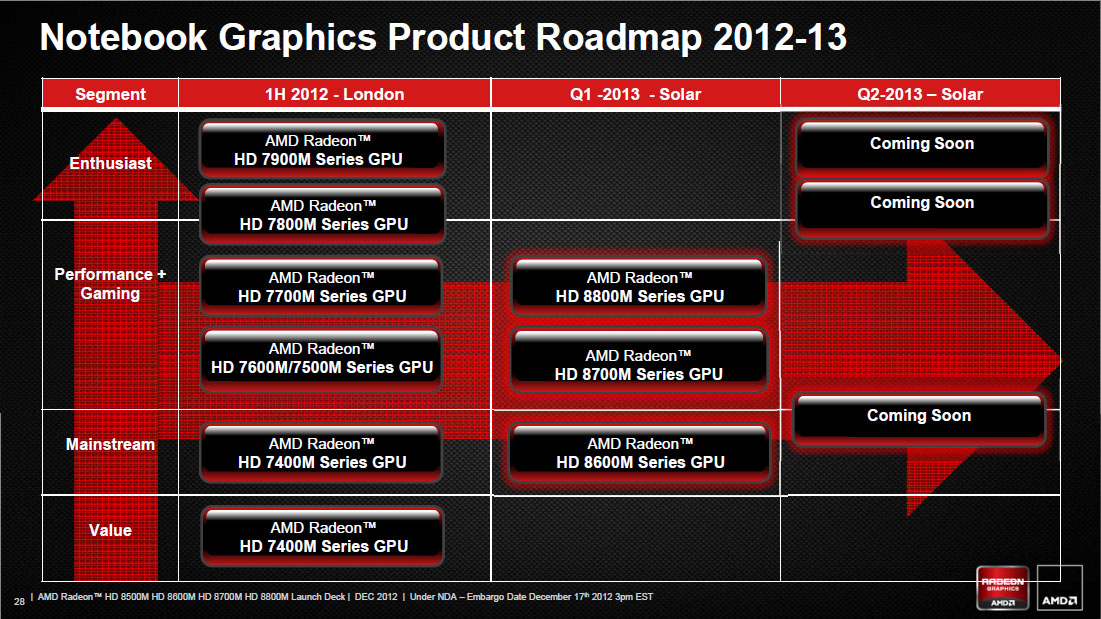
by Ryan Smith on January 8, 2013 12:15 AM ESTAlong with their announcement of their annual desktop GPU rebadge, AMD has also released the full product specifications for their new Radeon HD 8000M mobile GPUs. These GPUs were first announced back in December, but at the time AMD only gave us vague descriptions of each series with little-to-no information on the individual SKUs. Now with CES kicking into gear, we have the individual SKU information on hand.
| AMD Radeon 8800M Series GPU Specification Comparison | |||||
| AMD Radeon HD 8870M | AMD Radeon HD 8850M | AMD Radeon HD 8830M | |||
| Was | Variant Of 7800M | Variant Of 7800M | Variant Of 7800M | ||
| Stream Processors | 640 | 640 | 640 | ||
| Texture Units | 40 | 40 | 40 | ||
| ROPs | 16 | 16 | 16 | ||
| Core Clock | 725MHz | 575-725MHz | 575MHz | ||
| Boost Clock | 775MHz | 625-775MHz | 625MHz | ||
| Memory Clock | 4.5GHz GDDR5 / 2GHz DDR3 | 4.5GHz GDDR5 / 2GHz DDR3 | 2GHz DDR3 | ||
| Memory Bus Width | 128-bit | 128-bit | 128-bit | ||
| VRAM | 2GB | 2GB | 2GB | ||
| FP64 | 1/16 | 1/16 | 1/16 | ||
| Transistor Count | 1.5B | 1.5B | 1.5B | ||
| GPU | Heathrow | Heathrow | Heathrow | ||
| Manufacturing Process | TSMC 28nm | TSMC 28nm | TSMC 28nm | ||
| Architecture | GCN | GCN | GCN | ||
Starting at the top is the 8800M series, which is composed of a number of not-quite rebadges of 7800M parts. All of these GPUs are based on the Heathrow GPU (desktop name: Cape Verde), packing 640 Stream Processors along with 40 texture units and 16 ROPs. This is paired with 2GB of memory on a 128bit bus, with AMD using both GDDR5 and DDR3 depending on the specific SKU.
Other than being minor variations on existing AMD GPUs, these products also enable AMD’s Boost Clock technology for the first time in a mobile part. Boost Clock allows the GPU to turbo up to a higher clockspeed so long as the GPU is under its power and temperature limits, allowing AMD to scrape every bit of thermal headroom from their GPUs. This technology has been available on certain desktop GPUs for more than half a year, but this is the first time we’ve seen it on a mobile part. Notably, NVIDIA’s mobile parts do not feature NVIDIA’s equivalent technology (GPU Boost) despite the fact that they introduced the technology on the desktop first, so AMD is ahead of NVIDIA in this regard.
| AMD Radeon 8700M Series GPU Specification Comparison | ||||||
| AMD Radeon HD 8790M | AMD Radeon HD 8770M | AMD Radeon HD 8750M | AMD Radeon HD 8730M | |||
| Was | New | New | New | New | ||
| Stream Processors | 384 | 384 | 384 | 384 | ||
| Texture Units | 24 | 24 | 24 | 24 | ||
| ROPs | 8 | 8 | 8 | 8 | ||
| Core Clock | 850MHz | 775MHz | 620-775MHz | 650MHz | ||
| Boost Clock | 900Mhz | 825MHz | 670-825MHz | 700MHz | ||
| Memory Clock | 4.5GHz GDDR5 | 4.5GHz GDDR5 | 4GHz GDDR5 / 2GHz DDR3 | 2GHz DDR3 | ||
| Memory Bus Width | 128-bit | 128-bit | 128-bit | 128-bit | ||
| VRAM | 2GB | 2GB | 2GB | 2GB | ||
| FP64 | 1/16 | 1/16 | 1/16 | 1/16 | ||
| Transistor Count | ? | ? | ? | ? | ||
| GPU | Mars | Mars | Mars | Mars | ||
| Manufacturing Process | TSMC 28nm | TSMC 28nm | TSMC 28nm | TSMC 28nm | ||
| Architecture | GCN | GCN | GCN | GCN | ||
Below the 8800M series is the 8700M series, marking the introduction of AMD’s new Mars GPU. This is a 4th (and presumably final) first-generation GCN GPU, packing 384 stream processors, 24 texture units, and 8 ROPs. The 8700M is connected via a 128bit memory bus to 2GB of either GDDR5 or DDR3 depending on the SKU, and like the 8800M series also features AMD’s Boost Clock. Interestingly, all Mars products only offer a PCIe 8x bus instead of the GPU industry standard 16x. The performance difference on these lower-performance parts should be miniscule, but it’s an example of one of the ways AMD was able to achieve their smaller die size by reducing the number of pins that needed to connect to the GPU.
| AMD Radeon 8600M/8500M Series GPU Specification Comparison | ||||||
| AMD Radeon HD 8690M | AMD Radeon HD 8670M | AMD Radeon HD 8590M | AMD Radeon HD 8570M | |||
| Was | New | New | New | New | ||
| Stream Processors | 384 | 384 | 384 | 384 | ||
| Texture Units | 24 | 24 | 24 | 24 | ||
| ROPs | 8 | 8 | 8 | 8 | ||
| Core Clock | 775MHz | 775MHz | 620MHz | 650MHz | ||
| Boost Clock | 825MHz | 825MHz | 700MHz | 700MHz | ||
| Memory Clock | 4.5GHz GDDR5 | 2GHz DDR3 | 4.5GHz GDDR5 | 2GHz DDR3 | ||
| Memory Bus Width | 64-bit | 64-bit | 64-bit | 64-bit | ||
| VRAM | 1GB | 1GB | 1GB | 1GB | ||
| FP64 | 1/16 | 1/16 | 1/16 | 1/16 | ||
| Transistor Count | ? | ? | ? | ? | ||
| GPU | Mars | Mars | Mars | Mars | ||
| Manufacturing Process | TSMC 28nm | TSMC 28nm | TSMC 28nm | TSMC 28nm | ||
| Architecture | GCN | GCN | GCN | GCN | ||
Finally we have the 8600M and 8500M series. These are essentially cut-down Mars parts, halving the memory busses from 128bits wide to 64bits wide, and should significantly castrate performance in the process. The feature set and functional unit counts are otherwise identical to the 8700M series. The difference between the 8600M and 8500M series appears to come down to solely clockspeeds; the 8600M parts are clocked up to 775MHz, while the 8500M are clocked up to 620MHz/650MHz.
Source: AMD Radeon HD 8000M Specifications


15 Comments
View All Comments
lowlymarine - Tuesday, January 8, 2013 - link
EIGHT "different" GPUs differentiated exclusively by clock speeds and memory configuration? With ranges of clock speeds on some of those parts? Is there some requirement that GPU naming conventions must be actively consumer-hostile?scottjames_12 - Tuesday, January 8, 2013 - link
I agree that it is over the top, but at least the different clock speeds / bus widths are separated into different models (with the exception of the 8750 :/ ). I'd prefer that to having the same model number and a lucky dip on what clockspeeds/bus width/gddr type you get. Especially when most laptop vendors don't provide that much detail on what you are getting.Having this many variants is obviously necessary to meet different cost points and TDP envelopes.
Beenthere - Tuesday, January 8, 2013 - link
Yes it's important to have consumer-hostile naming conventions in all graphics cards, just as it's necessary to have tit and arse graphics on GPU cards and boxes. How do you expect to stimulate sales from the 13 year olds?CeriseCogburn - Monday, January 14, 2013 - link
AMD is guilty of the sex box sales. Not nVidia.bstulic - Thursday, February 21, 2013 - link
http://todayswall.com/files/imagecache/1680x1050/d...usteg - Tuesday, January 8, 2013 - link
"Notably, NVIDIA’s mobile parts do not feature NVIDIA’s equivalent technology (GPU Boost) despite the fact that they introduced the technology on the desktop first, so AMD is ahead of NVIDIA in this regard."I'm pretty sure the Kepler-based Mobile cards have Boost; I have a Geforce GT645M and Boost is enabled by default.
Death666Angel - Tuesday, January 8, 2013 - link
That's what I get when I do some googling as well and in the Alienware M17x-R4 review it says of the GTX680M: "The core clock now runs at only 719MHz with a boost clock of 758MHz[...]"CeriseCogburn - Monday, January 14, 2013 - link
Ahh, the gigantic article error that will NEVER be corrected because of course it's a lie against nVidia.I don't see the fixed thanks response here we usually see.
Nope, no amd bias here. I was wrong all along.
roll eyes
silverblue - Tuesday, January 8, 2013 - link
...the lack of any news on the 8900M series is disappointing.I am concerned that AMD usually leaves their parts ROP-limited, though here, with such a narrow memory interface, I suppose it's not really going to be a bottleneck.
silverblue - Tuesday, January 8, 2013 - link
They currently read "4.5Hz GDDR5"; missing a G.