Change of Strategy: A New GlobalFoundries CEO in Dr. Thomas Caulfield
by Anton Shilov on March 15, 2018 1:00 PM EST- Posted in
- Semiconductors
- GlobalFoundries
- IBM
- 7nm
- FD-SOI
- 5nm
- 12FDX
- 22FDX
GlobalFoundries: Manufacturing Capacities
A portfolio of competitive process technologies is only a part of the equation when it comes to contract manufacturing of semiconductors and the foundry businesss. You have to be able to produce chips in high volumes and meet demands of your customers. As such, during his tenure at GlobalFoundries, Sanjay Jha invested in various fabs to increase their production capacities.
| GlobalFoundries' 2017 Expansion Plans | |||||||
| Process Technologies current and planned |
Current Capacity* wafer starts per month |
Planned Increase | Target Capacity* wafer starts per month |
Target Timeframe | |||
| Fab 1 (Dresden, Germany) |
32 nm SOI 28 nm 22FDX (FD-SOI) 12FDX (FD-SOI) |
up to 80,000 | +40% | ~110,000 | 2020 | ||
| Fab 7 (Singapore) |
130 nm 65/55 nm 40 nm RF-SOI |
68,000 | +35% for 40 nm | Over 68,000 | 2017~2018 | ||
| Fabs (Singapore) |
180 nm | unknown | +?% for 180 nm | unknown | 2017~2018 | ||
| Fab 8 (New York, USA) |
14LPP 7 nm |
up to 60,000 | +20% for 14LPP | Over 60,000 | Early 2018 | ||
| Fab 9 (New York, USA) |
RF-SOI 90 - 350nm |
unknown | +?% for RF-SOI | 40,000** | 2016 | ||
| Fab 11 (Chengdu, China) | 180/130 nm 22FDX (FD-SOI) |
- | - | Ph. 1: 20,000 Ph. 2: 65,000 P1+P2: 85,000 |
Ph. 1: 2018+ Ph. 2: 2019+ |
||
| *Please note that actual wafer starts per month (WSPM) output of a fab depends on multiple factors, including process technologies used. As a result, all the WSPM capacity numbers are relative and may not reflect actual performance. Keep in mind, that as foundries and IDMs increase usage of multi-patterning techniques, their effective WSPM output drops as wafers spend more time in the cleanroom. Hence, to keep the wafer starts per month capacity, chipmakers need to add equipment (which may, or may not, involve physical expansion of the cleanroom space).
** 200-mm wafers. |
|||||||
Following the Fab 8 upgrades initiated by Ajit Manocha in 2013, GlobalFoundries announced a $55-million upgrade plan for the Fab 9 (a 200-mm fab in Essex Junction, Vermont, that belonged to IBM). This is the primary home of GF’s RF-SOI production, and the update is to increase its capacity to 40,000 wafer starts per month (WSPM). In early 2017, GlobalFoundries announced a major effort to increase capacities of the company’s existing fabs. In addition, last year the company started to build a new fab near Chengdu, China.
The most recent upgrades of Fab 8 were driven by intention to maximize its output and boost its peak WSPM capacity in the light of quad-patterning usage by the 7LP process technology. As a private company, GlobalFoundries does not comment on its existing production capacities (i.e., we do not know whether the Fab 8 upgrades have been completed or not), but only says that everything has been going on as planned.
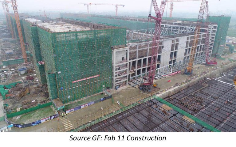
Meanwhile, GlobalFoundries’ plans to expand FD-SOI capacity of the Fab 1 by 40% by 2020 clearly indicate that the company pins a lot of hopes on FD-SOI and expects more customers to jump on this bandwagon. For the same reason, the company is building up the Fab 11 near Chengdu: China is among the world’s largest consumers of microelectronics and therefore its local chip development industry is expected to thrive in the coming years. Offering those IC designers an inexpensive low-power process technology locally is potentially a very good plan that puts GlobalFoundries ahead of SMIC and UMC (who both yet have to develop something that would be competitive against the 22FDX).
Sanjay Jha’s GlobalFoundries: From $4.1 to $6.2 Billion
While construction and upgrades usually proceed smoothly, they tend to cost a lot. In fact, GlobalFoundries has been expanding and upgrading throughout its history, which caused rather extreme spending. In fact, according to Mubadala’s financial reports, GlobalFoundries has been losing money throughout its history on various projects and has never been profitable.
Sanjay Jha has managed to land a variety of new customers and increase GlobalFoundries’ sales of semiconductor wafers from approximately $4.1 billion in 2013 to $6.2 billion in 2017 (the latter figure comes from Ahmed Al Idrissi, chairman of GlobalFoundries, but it has not been published yet). Mr. Jha has also succeeded in cutting down GF’s losses from $1.5 billion in 2014 to $427 million in 2016. However, the announced upgrades, procurement of new tools, and construction of the new fab near Chengdu naturally increased capital expenditures in 2017: the company’s losses in the first half of the year totaled ~$581 million (up from $427 million for the whole year 2016).

It is noteworthy that GlobalFoundries still has an option to further expand its Fab 8 by building the so-called Fab 8.2 module adjacent to the existing Fab 8.1 and TDC (technology development center). The company reached an agreement about the construction with the Saratoga County Industrial Development Agency back in 2013, but has never exercised the option.
Related Reading
- The Future of Silicon: An Exclusive Interview with Dr. Gary Patton, CTO of GlobalFoundries
- GlobalFoundries Adds 12LP Process for Mainstream and Automotive Chips; AMD Planning 12LP CPUs & GPUs
- GlobalFoundries Weds FinFET and SOI in 14HP Process Tech for IBM z14 CPUs
- GlobalFoundries Details 7 nm Plans: Three Generations, 700 mm², HVM in 2018
- GlobalFoundries to Expand Capacities, Build a Fab in China
- GlobalFoundries Updates Roadmap: 7 nm in 2H 2018, EUV Sooner Than Later?
- AMD Amends GlobalFoundries Wafer Supply Agreement Through 2020, Gaining New Flexibility & New Costs


14 Comments
View All Comments
ZolaIII - Thursday, March 15, 2018 - link
Well not a really interesting article...How about writing more about 14HP FinFET-SOI & beyond.
III-V - Thursday, March 15, 2018 - link
Ah yes, FDSOI... the transistor vaporware. Real interesting stuff, there...ZolaIII - Thursday, March 15, 2018 - link
I told 14HP which is 14nm FinFET structure on SOI wafer and beyond 14nm... FD-SOI is hire to stay & badly needed for G5, mimo x4 in mobile, IoT and cetera basically all RF blocks & CMOS on it is coming too.BestGuess - Thursday, March 15, 2018 - link
The article states that 14HP is a descendant of 14LP from Samsung, but more likely it is a marriage of IBM's internally developed 14nm SOI process and 14LP. See IBM's last publication on it prior to the acquisition:http://ieeexplore.ieee.org/abstract/document/70469...
The descriptions of IBM's Power9 chips, which indicate it is SOI and features embedded DRAM, sure look a lot more like the IBM technology than the bulk 14LP technology...
As for RFCMOS applications, FDSOI could be a game changer, since as a planar technology, it doesn't suffer from the high gate capacitance of Finfets. This capacitance is part of the Finfet advantage for Logic applications, but is a real handicap for RF, which requires dealing with much higher frequencies.
ZolaIII - Thursday, March 15, 2018 - link
Yes I reed that article long time ago so do I really need to quote my self again? 14HP FinFET-SOI and beyond.GF 22 nm FD-SOI isn't game changer but a winning design & for digital it's proven how it can match the best efforts on 10 nm FinFET regarding power consumption when back biasing is used that is 0.4V (for small to medium sized SoC's) while analogue where it's obviously only logical choice goes with 0.8V. For most things & especially IoT you need to use combined multi RF & digital components in the same package & that it's both development and final product price is cheap so it's absolute design win for both RF and IoT and good enough for mainstream, it's also win for DSP's not so much for FPGA's & GPU's as they tend to be huge but in smaller or mobile ones it still wins because of its price. Only thing where it loses is HPC & desktop CPU which tend to push operating frequencies as much as possible & FinFET is better at this...
Cooe - Thursday, March 15, 2018 - link
I'm happy with this choice. IBM produces great tech executives. Just look at Lisa Su.TheJian - Saturday, March 17, 2018 - link
You must be kidding. They should have kept Dirk Meyer who said in 2011, we need to make a KING product in cpu/gpu FIRST, then do this APU/console crap that has junk margins that are merely additive, rather than the bulk of your net income. You can use junk like that to milk your tech for the last few dollars but like NV/Intel, AMD should be concentrating on the enterprise stuff or rich people PERIOD. After that leaves cards or chips on the shelf, THEN and ONLY then do you chase the low margin products.If you are limited in supply (can't produce them as fast as you sell them I mean), which is the case for both AMD/NV currently, you shouldn't be wasting time on 10-20% margins (which for AMD just means barely break even on a good quarter), but rather you should be chasing 50%+ margins.
For anyone who doesn't believe this is how things work (they fired Dirk for saying it...LOL, morons), you should just compare the last decade of NV & Intel quarterly reports to AMD's. Note Intel plops chips on TOP of their stack when adding new models (HEDT anyone?), and NV simply put out 1080/1070 (for example) and took a year to put out a 1060. No point in wasting silicon on poor people (sorry, just the facts) when you can nab a RICH person who has throw away cash sitting all around him and upgrades yearly :) At anything under 30% margins AMD just ends up barely paying interest on their debt, wafer agreement penalties etc. They need to hit 40%+ before they start rolling in cash. They should have hit servers first, then home users. IE, I'd rather be chasing $1000-7000 cpus if I was AMD instead of chasing <$1000. They just put out an APU that has a max price currently of $169...ROFLMAO. Lisa should be fired (and most of their management, they are clueless), and Dirk should be sought out ASAP. He was right. Well, DUH.
Now worse IMO, they are giving Intel IP, instead of MAKING THAT CHIP THEMSELVES! Intel will probably charge $400+ for the 8809g. That should have been AMD. AMD is probably making peanuts on that, while Intel takes the bulk of the profits. If I was AMD's CEO I'd fire anyone who brought me an idea that didn't make 40%+ margins out of the gate at least. Intel/NV are chasing 60% stuff and higher. They'd be 70% margins overall if they axed the bottom...LOL.
Not a knock on IBM people, just on this person. Letting Intel/NV have the high end for basically most of the last 7yrs, is retarded. Consoles killed R&D that should have kept them in the cpu race, and drop watts/heat on products, allowed proper R&D to not have crap launches with problem after problem (mboards not having bios' finished, memory issues, vid cards launching and having to speed up fans to mitigate issues etc). With anyone but a fanboy, you probably only get ONE chance to impress your customers. You can't screw up a launch if you're the little guy, you need to get that right out of the gate. Who's idea was it to launch a month or two early damaging the cpu launch? Not the Motherboard makers...AMD had ~800mil to survive one more month (one more year easily), so why push the launch too early? You're fired. Who chose SINGLE DIGIT console margins for 2yrs (they finally said mid double digits-meaing 15% or less or you'd say 16+ right?), instead of CPU/GPU/DRIVERS R&D? You're fired too. Who chose HBM not once, but TWICE, when it was worth nothing more than a buzzword as that bandwidth was not needed at all (see NV cards). It still isn't needed now either which is why all NV home cards have GDDR5x or less, and why their margins are GREAT and setting record profits/margins/revenue quarter after quarter. Who decide a buzzword was worth the risk of massive shortages and super high BOM costs which kills margins (and card supply). If you can't get it on a shelf, your tech is useless. NV chose the KISS principle. For AMD management, who'm I'm sure hasn't heard of this (LOL), it stands for KEEP IT SIMPLE STUPID. AMD went hard to produce, wasteful (overkill bandwidth when only unicorns were using 4K...LOL) and expensive. NV chose easy to make, cheap, and adequate for even Titan. Again AMD management, do you read quarterly reports (your own, and your competition?)?? No? You're fired. Come back when you understand basic economics. Price wars as the only broke guy in the room?? LOL. I digress.
zodiacfml - Saturday, March 17, 2018 - link
If it was that easy, they did just what you said, with pleasure.However, AMD's technical ability can't keep up with Intel and Nvidia. Therefore, it has always been AMD's last resort to choose better memory for performance gain to keep up. This is the reason why AMD has been first with integrated memory controllers, HBM, and choosing higher bandwidth memory spec for some cards vs. competing cards of Nvidia
They're pretty lucky with this as the cryptocurrency ethash/Ethereum algorithm is memory intensive, making their cards superior for mining despite behind in gaming performance or other crypto algorithms. It should have been a quick fix for their profitability by producing more cards but they are limited by the shortage of memory.
Thermalzeal - Friday, April 6, 2018 - link
AMD Can't keep up? That is the most interesting thing that causes my eyebrow to raise, that has been said in a long time :P It's a full stack of technical implementation and AMD has led the market in pushing the tech forward while Intel has bunny suits and disparate architectures for rich people.I honestly can't stand Intel Fanboys, sure if you actually flex your computational power in a single socket you can drain your capex like a cray (see what I did there) but truly if you want to zen out and achieve more sustainable opex AMD has been a leader.
Intel has only achieved it's success with 25x pockets. So, I really don't think any respect is due to Intel Engineers for marketshare that is complete hogwash. AMD has always done more with less, and unfortunately had complete useless humans like Hector Ruinz destroy the company and Global Foundries.
Galcobar - Thursday, March 15, 2018 - link
"Sanjay Jha, who lead the world’s..."Led.
Past tense of the verb lead is led. Not that English makes it easy since the pronunciation for the noun lead is the same as the past tense verb led.