HiSilicon Kirin 970 - Android SoC Power & Performance Overview
by Andrei Frumusanu on January 22, 2018 9:15 AM EST
Today I would say that there’s only two truly vertically integrated mobile OEMs who have full control over their silicon: Apple and Huawei – and of the two one could say Huawei is currently even more integrated due to in-house modem development. Huawei’s semiconductor division, HiSilicon, has over the last several years been the one company which seems to have managed what the others haven’t: break in into the high-end market with solutions that are competitive with the current leader in the business, Qualcomm.
I remember the Honor 6 with the newly branded (Previously not having any “halo” line-up name) Kirin 920 SoC as the first device with the company’s in-house SoC that we reviewed. These and the following generation the Kirin 930 suffered from immaturity with problems such as a very power hungry memory controller and very disappointing camera processing pipeline (ISP/DSP). The Kirin 950 was in my opinion a turning point for HiSilicon as the product truly impressed and improved the quality of the product, catching many eyes in the semiconductor industry, including myself in the resulting review of the Huawei Mate 8.
Over the last several years we’ve seen great amounts of consolidation in the mobile semiconductor industry. Companies such as Texas Instruments which were once key players no longer offer mobile SoC products in their catalogue. We’ve seen companies such as Nvidia try and repeatedly fail at carving out meaningful market-share. MediaTek has tried providing higher end SoCs with the Helio X line-up with rather little success to the point that the company has put on hold development in that segment to rather focus on higher margin parts in the P-series.
Meanwhile even Samsung LSI, while having a relatively good product with its flagship Exynos series, still has not managed to win over the trust of the conglomorate's own mobile division. Rather than using Exynos as an exclusive keystone component of the Galaxy series, Samsing has instead been dual-sourcing it along with Qualcomm’s Snapdragon SoCs. It’s therefore not hard to make the claim that producing competitive high-end SoCs and semiconductor components is a really hard business.
Last year’s Kirin 960 was a bit of a mixed bag: the SoC still delivered good improvements over the Kirin 950 however it was limited in terms of what it could achieve against competing flagship SoCs from Samsung and Qualcomm as they both had a process node advantage. Huawei's introduction of flagships with new generation of SoCs in the fourth quarter is more close to the release time-frame of Apple than the usual first quarter that we’ve come accustomed of Qualcomm and Samsung.
As such when pitting the Kirin versus Snapdragon and Exynos’s we’re looking at a product that’s more often than not late to the party in terms of introduction of new technologies such as process node and IP. The Kirin 970 fits this profile: as a 10nm Cortex-A73 generation-based SoC, it lagged behind Qualcomm and Samsung in terms of process node, yet being too early in its release to match up with ARM’s release schedule to be able to adopt DynamiQ and A75 and A55 based CPU cores for this cycle. That being said the Kirin 970 enjoys a few months with technical feature parity with the Snapdragon 835 and Exynos 8895 before we see new Snapdragon 845 and Exynos 9810 products later in the usual spring refresh cycle.
Nevertheless, the article today is a focus on the Kirin 970 and its improvements and also an opportunity to review the current state of SoCs powering Android devices.
| HiSilicon High-End Kirin SoC Lineup | |||
| SoC | Kirin 970 | Kirin 960 | Kirin 950/955 |
| CPU | 4x A73 @ 2.36 GHz 4x A53 @ 1.84 GHz |
4x A73 @ 2.36GHz 4x A53 @ 1.84GHz |
4x A72 @ 2.30/2.52GHz 4x A53 @ 1.81GHz |
| GPU | ARM Mali-G72MP12 746 MHz |
ARM Mali-G71MP8 1037MHz |
ARM Mali-T880MP4 900MHz |
| LPDDR4 Memory |
4x 16-bit CH LPDDR4 @ 1833 MHz 29.9GB/s |
4x 16-bit CH LPDDR4 @ 1866MHz 29.9GB/s |
2x 32-bit LPDDR4 @ 1333MHz 21.3GB/s |
| Interconnect | ARM CCI | ARM CCI-550 | ARM CCI-400 |
| Storage I/F | UFS 2.1 | UFS 2.1 | eMMC 5.0 |
| ISP/Camera | Dual 14-bit ISP | Dual 14-bit ISP (Improved) |
Dual 14-bit ISP 940MP/s |
| Encode/Decode | 2160p60 Decode 2160p30 Encode |
2160p30 HEVC & H.264 Decode & Encode 2160p60 HEVC Decode |
1080p H.264 Decode & Encode 2160p30 HEVC Decode |
| Integrated Modem | Kirin 970 Integrated LTE (Category 18/13) DL = 1200 Mbps 5x20MHz CA, 256-QAM UL = 150 Mbps 2x20MHz CA, 64-QAM |
Kirin 960 Integrated LTE (Category 12/13) DL = 600Mbps 4x20MHz CA, 64-QAM UL = 150Mbps 2x20MHz CA, 64-QAM |
Balong Integrated LTE (Category 6) DL = 300Mbps 2x20MHz CA, 64-QAM UL = 50Mbps 1x20MHz CA, 16-QAM |
| Sensor Hub | i7 | i6 | i5 |
| NPU | Yes | No | No |
| Mfc. Process | TSMC 10nm | TSMC 16nm FFC | TSMC 16nm FF+ |
The Kirin 970, isn't a major IP overhaul as it continues to use the same central processing unit IP from ARM that was used in the Kirin 960. The new SoC even doesn't improve the frequency of the CPU clusters as we still see the same 2.36GHz for the A73 cores and 1.84GHz for the A53 cores. When ARM originally launched the A73 we had seen optimistic targets of up to 2.8GHz on TSMC 10nm, but we seem to have largely missed that target, a sign of ever increasing difficulty to scale frequency in mobile SoCs as the diminishing returns from process node updates become worse and worse.
The Kirin 970 does bring a major overhaul and change in the GPU configuration as we see the first implementation of ARM’s Mali G72 in a 12-cluster configuration, a 50% increase in core count over the Kirin 960’s G71-MP8 setup. The new GPU is running at a much reduced frequency of 746MHz versus the 1033MHz of the Kirin 960. In Matt Humrick’s review of the Kirin 960 we saw some disastrous peak average power figures of the Mali G71 outright exploding the thermal envelope of the Mate 9, so hopefully the architectural improvements of the new G72 alongside a wider and lower clocked configuration in conjunction with the new process node will bring significant improvements over its predecessor.
The new modem in the Kirin 970 now implements 3GPP LTE Release 13 and supports downlink speeds of up to 1200Mbps thanks to up to 5x20MHz carrier aggregation with 256-QAM, making the new Kirin modem feature equivalent to Qualcomm’s X20 modem that’ll be integrated in the Snapdragon 845.
The big story surrounding the Kirin 970 was the inclusion of a dedicated neural processing unit. The NPU, as HiSilicon decided to name it, is part of a new type and generation of specialised dedicated acceleration blocks with the aim of offloading “inferencing” of convolutional neural net (CNNs). Many will have heard buzzwords such as artificial intelligence surrounding the topic, but the correct term is machine learning or deep learning. The hardware acceleration blocks with various names from various companies do not actually do any deep learning, but rather are there to improve execution (inferencing) of neural network models while the training of the models will still remain something that will be done either in the cloud or by other blocks in the SoC such as the GPU. It’s still the early days but we’ll have a proper look at the NPU in its dedicated section of the article.
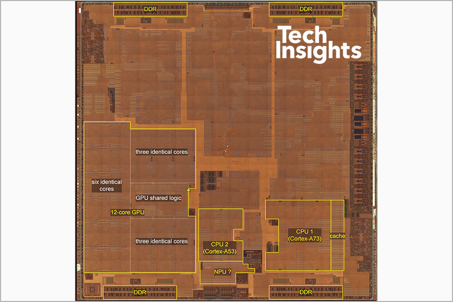
SoC die shot image & labels courtesy of TechInsights Mate 10 teardown
As aforementioned one of the bigger improvements of the Kirin 970 is the switch to a TSMC 10FF manufacturing node. While 10nm is supposed to be a long-lived node for Samsung's foundry – where indeed we’ll see two full generations of SoCs produced on 10LPE and 10LPP – TSMC is taking a different approach and sees its own 10FF process node a short-lived node and stepping-stone to the much anticipated 7FF node, which is to be introduced later in 2018. As such the only TSMC 10FF mobile products to date have been the low-volume MediaTek X30 and Apple 10X in summer and the high-volume Apple A11 and HiSilicon Kirin 970 in Q3-Q4, a 2-3 quarter after Samsung had entered high-volume production of the Snapdragon 835 and Exynos 8895.
HiSilicon’s expectations of the new process node are rather conservative improvement of only 20% in efficiency at the same performance point for the apples-to-apples CPU clusters, below ARM’s earlier predictions of 30%. This rather meagre improvement in power will be likely one of the reasons why HiSilicon decided not to increase the CPU clocks on the Kirin 970, instead focusing on bringing down power usage and lowering the TDP when compared to the Kirin 960.
The SoC does enjoy a healthy die size shrink from 117.72mm² down to 96.72mm² even though the new SoC has 50% more GPU cores as well as new IP blocks such as the NPU. Our colleagues at TechInsights have published a detailed per-block size comparison between the Kirin 960 and Kirin 970 and we see a 30-38% decrease in block size for apples-to-apples IP. The Cortex-A73 quad-core cluster now comes in at only 5.66mm², a metric to keep in mind and in stark contrast to Apple which is investing twice as much silicon area in its dual-core big CPU cluster.


116 Comments
View All Comments
zorxd - Monday, January 22, 2018 - link
Samsung isn't vertically integrated? They also have their own SoC and even fabs (which Huawei and Apple don't)Myrandex - Monday, January 22, 2018 - link
Agreed, but they don't even always use their own components like Huawei and Apple do, I think I've yet to own a Samsung Smartphone that uses a Samsung SoC. I think they will eventually get there though although I can't say I have any idea why they aren't doing it today.jospoortvliet - Saturday, January 27, 2018 - link
Samsung always uses their own SOCs unless they are legally forced not to, like in the US...levizx - Saturday, January 27, 2018 - link
They are DEFINITELY NOT legally forced to use Qualcomm chips in China, especially for the worlds biggest carrier China Mobile. As for the US, if Huawei is not forced to use Qualcomm, I can't imagine why Samsung would unless they signed a deal with Qualcomm - then again that's just by choice.Andrei Frumusanu - Monday, January 22, 2018 - link
Samsung's mobile division (which makes the phones) still makes key use of Snapdragon SoCs for certain markets. Whatever the reason for this and we can argue a lot about it, fact is that the end product more often than not ends up being as the lowest common denominator in terms of features and performance between the two SoC's capabilities. In that sense, Samsung is not vertically integrated and does not control the full stack in the same way Apple and Huawei do.Someguyperson - Monday, January 22, 2018 - link
No, Samsung simply isn't so vain as to use it's own solutions when they are inferior. Samsung skipped the Snapdragon 810 because their chip was much better. Samsung used the 835 instead of their chip last year because the 835 performed nearly exactly the same as the Samsung chip, but was smaller, so they could get more chips out of an early 10 nm process. Huawei chooses their chips so they don't look stupid by making an inferior chip that costs more compared to the competition.Samus - Monday, January 22, 2018 - link
Someguyperson, that isn't the case at all. Samsung simply doesn't use Exynos in various markets for legal reasons. Qualcomm, for example, wouldn't license Exynos for mobile phones as early as the Galaxy S III, which is why a (surprise) Qualcomm SoC was used instead. Samsung licenses Qualcomm's modem IP, much like virtually every SoC designer, for use in their Exynos. The only other option has historically been Intel, who until recently, made inferior LTE modems.I think it's pretty obvious to anybody that if Samsung could, they would, sell their SoC's in all their devices. They might even sell them to competitors, but again, Qualcomm won't let them do that.
lilmoe - Monday, January 22, 2018 - link
Since their Shannon modem integration in the Exynos platform, I struggled to understand why...My best guess would be a bulk deal they made with Qualcomm in order for them to build Snapdragons on both their 14nm and 10nm. Samsung offered a fab deal, Qualcomm agreed to build using Samsung fabs and provide a generous discount in Snapdragon resale for Galaxies, but in the condition to buy a big minimum amount of SoCs. That minimum quantity was more than what was needed for the US market. Samsung did the math, and figured that it was more profitable to keep their fabs ramped up, and save money on LTE volume licensing. So Samsung made a bigger order and included Chinese variants in the bulk.
I believe this is all a bean counter decision, not technical or legal.
KarlKastor - Thursday, January 25, 2018 - link
That's easy to answer. Samus is right, it's a legal problem. The reason is named CDMA2000.Qualcomm owns all IP concerning CDMA2000.
Look at the regions where a Galaxy S is shipped with a Snapdragon and look a the Countries using CDMA2000. That's North America, Chna and Japan.
Samsung has two choices: Using a Snapdragon SoC with integrated QC Modem or plant a dedicated QC Modem alongside their own SoC.
The latter is a bad choice concerning space and i think it's more expensive to buy an extra chip instead of just using a Snapdragon.
I bet all this will end when Verizon quits CDMA2000 in late 2019 and Samsung will use their Exynos SoCs only. CDMA200 is useless since LTE and is just maintained for compatibility reasons.
In all regions not using this crappy network, Samsung uses Exynos SoCs in every phone from low cost to high end.
So of course Samsung IS vertically integrated. Telling something else is pretty ridicoulous.
They have theor own fabs, produce and develope their own SoC, modem, DRAM and NAND Flash and have their own CPU and modem IP. They only lack their own GPU IP.
So who is more vertically integrated?
KarlKastor - Thursday, January 25, 2018 - link
I forgot their own displays and cameras. Especially the first is very important. The fact, that they make their own displays enabled more options in design.Think of their Edge-Displays, you may like them or not, but with them the whole design differed much from their competitors.