The Intel Lakefield Deep Dive: Everything To Know About the First x86 Hybrid CPU
by Dr. Ian Cutress on July 2, 2020 9:00 AM ESTHow To Treat a 1+4 Hybrid CPU
At the top of the article, I explained that the reason for using two different types of processor core, one big on performance and the other big on efficiency, was that users could get the best of both worlds depending on if a workload could be run efficiently in the background, or needed the high performance for a user experience interaction. You may have caught onto the fact that I also stated that because Intel is using a 1+4 design, it actually makes more sense for multi-threaded workloads to run on the four Atom cores.
Using a similar power/performance graphs, the effect of having a 1+4 design is quite substantial. On the left is the single core power/performance graphs, but on the right is when we compare 1 Sunny Cove to all 4 Tremont cores working together.
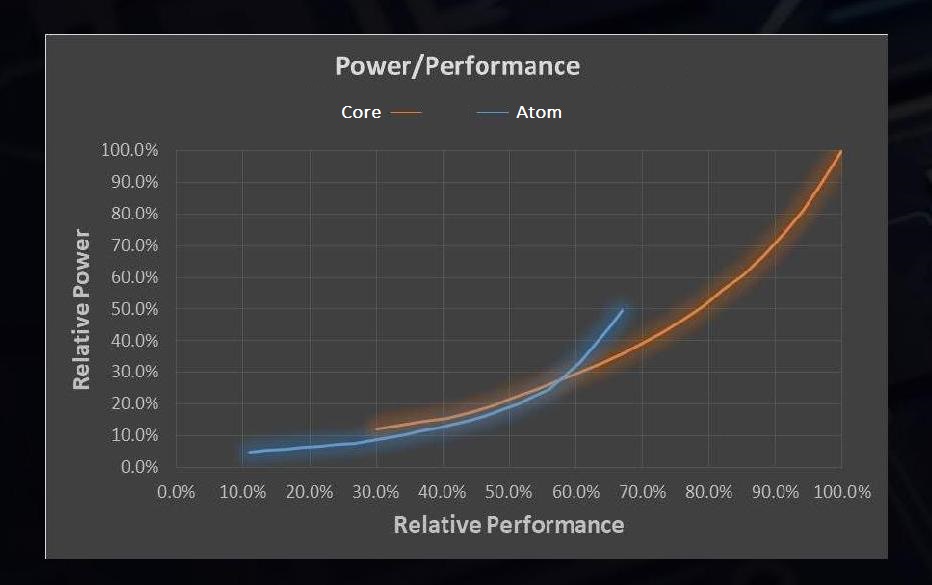
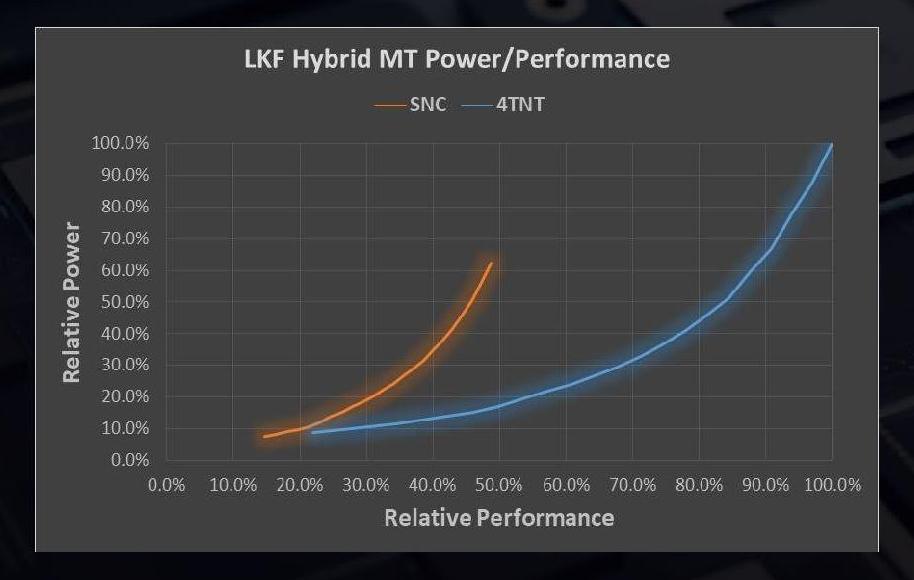
Where the previous graph considered a 1+1 design, which is more relevant in those user experience scenarios listed above, on the right is the 1+4 design for when the user demands a heavier workload that might not be latency critical. Because there are four Atom cores, the blue line multiplies by four in both directions.
Now obviously the real world scenario is somewhere between the two, as it is possible to use only one, two, or three of the smaller cores at any given time. The CPU and the OS is expected to know this, so it can govern when workloads that can be split across multiple cores end up on either the big core or the small core.
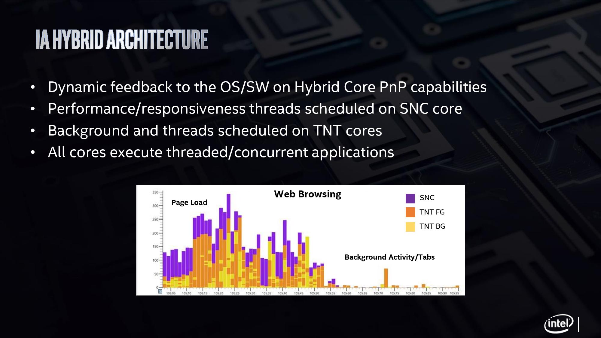
In this graph from Intel, we have three distinct modes on which threads can operate.
- ‘Sunny Cove/SNC’ is for responsiveness and user experience threads,
- ‘Tremont/TNT Foreground’, for user related tasks that require multiple threads that the user is waiting on.
- ‘Tremont/TNT Background’, for non-user related tasks run in efficiency mode
Even though the example here is web browsing, it might be best to consider something a bit beefier, like video encoding.
If we run video encoding, because it is a user related task that requires multiple threads, it will run on the four Tremont cores (TNT FG). Anything that Windows wants to do alongside that gets scheduled as TNT BG. If we then open up the start menu, because that is a responsiveness task, that gets scheduled on the SNC core.
Is 1+4 the Correct Configuration?
Intel here has implemented a 1+4 core design, however in the smartphone space, things are seen a little differently. The most popular configuration, by far, is a 4+4 design, simply because a lot of smartphone code is written to take advantage of multiple foreground or multiple background threads. There are a number of cost-down designs that reduce die area and power by going for a 2+4 implementation. Everyone seems adamant that 4 is a good number for the smaller cores, partly because they are small and cheap to add, but because Arm’s quad-core implementation is a base unit for its IP.
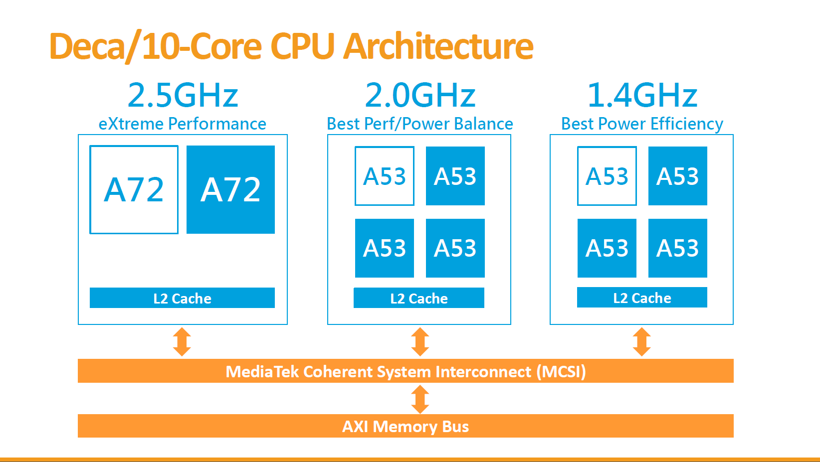
The smartphone space in recent quarters has also evolved from a two tier system of cores. In some of the more leading edge designs, we now have three types of core: a big, a middle, and a small. Because of the tendency to stay with eight core designs, we now get 1+3+4 or 2+2+4 designs, powered by complex schedulers that manage where to put the threads for the best user experience, the best battery life, or somewhere in the middle. Mediatek has been famously dabbling in 10 core designs, going for a 2+4+4 approach.
One thing missing from all of these implementations is an SoC with one big core and four small cores. Smartphone vendors don’t seem to be interested in 1+4 silicon, and yet Intel has decided on it for Lakefield. This is borne out of decisions made on both sides.
From the smartphone perspective, when hybrid designs came about, the big cores just weren’t powerful enough on their own. In order to offer something more than simply basic, at least two cores were needed, but because of how Arm architected the big and little designs, it almost became standard to look into 4+4 implementations of big and small cores. It was only until this configuration was popularized over a couple of years, and Arm big cores got more powerful, that chip designs started looking at 2+4, or 1+3+4 designs.
On Intel’s side of the fence, the biggest problem it has is the size of the Sunny Cove core. By comparison, it’s really, really big. Because the graphics core is the same as Ice Lake and reuses its design, there simply isn’t enough room within the 82 mm2 compute die to add another core. Not only that, but there is a question of power. Sunny Cove wasn’t built for sub-1W operation, even in the Tremont design. We see big smartphone silicon pulling 4-5W when all eight cores are active – there is no way, based on our understanding of Intel’s designs, that we could see four (or even two) Sunny Cove cores being in the optimal performance per watt range while being that low. Intel’s Lakefield graphics, with 64 EUs, is running at only 500 MHz – a lot lower than the Ice Lake designs. Even if Intel moved that down to a 32 EU design to make space for another Sunny Cove core, I reckon that it would eat the power budget for breakfast and then some.
Intel has made the 1+4 design to act as a 0+4 design that sometimes has access to a higher performance mode. Whereas smartphone chips are designed for all eight cores to power on for sustained periods, Lakefield is built only for 0+4 sustained workloads. And that might ultimately be its downfall. This leads onto a deep discussion about Lakefield’s performance, and what we should expect from it.


221 Comments
View All Comments
returnzer0 - Friday, July 3, 2020 - link
So no, they did not, in fact, read the same article.s.yu - Monday, July 6, 2020 - link
Mystery solved!vanilla_gorilla - Friday, July 3, 2020 - link
https://www.anandtech.com/show/15877/intel-hybrid-..."At the top is the single Sunny Cove core, also present in Ice Lake. Intel has stated that it has physically removed the AVX-512 part of the silicon, however we can still see it in the die shot. This is despite the fact that it can’t be used in this design due to one of the main limitations of a hybrid CPU. We’ll cover that more in a later topic."
It was NOT physically removed but it cannot be used so it doesn't really matter. In practice this will have no AVX-512.
dotjaz - Friday, July 3, 2020 - link
Also "However, all modern software assumes a homogeneous processor", that's why they have to support exactly the same ISA extensions. I didn't realise Windows is the only modern software in existence.Meteor2 - Friday, July 3, 2020 - link
Why so rude, dotjaz?dotjaz - Saturday, July 4, 2020 - link
So which part is rude? Is this rude asking you what's rude? Sorry your feelings got hurt. There, happy now?jospoortvliet - Sunday, July 5, 2020 - link
Linux also expects it. Modern enough?jeremyshaw - Thursday, July 2, 2020 - link
Good. This action ensures this segment of products will be easier to emulate on arm, helping to tear these products away from Intel's grasp.Kangal - Sunday, July 5, 2020 - link
To be honest, this is a great innovation.It's just the execution is quite lacking, and on top of that, it's a couple years too late.
Just imagine a SoC such as:
3x Big processor (Intel Core M), eg/ Core i7-8500Y
5x Small processor (Intel Atom), eg/ Atom x7-Z8750
Dynamic Scaling:
(Idle) 4x Small Cores run at 500MHz at Idle
(Very-low power) 4x Small Cores clock starting at 1.0GHz
(Low-power use) 5x Small Cores clock upto 2.5GHz
(Medium power) 3x Big Cores starting at 1.5GHz, 5x Small Cores upto 2.5GHz
(Regular power) 3x Big Cores at 2.0GHz, 5x Small Cores at 2.0GHz
(High-power use) 3x Big Cores at 3.0GHz, 5x Small Cores at 2.0GHz
(Very-high power) 3x Big Cores at 4.0GHz, 5x Small Cores at 2.5GHz
(Max-power use) 1x Big Cores at 5.0GHz, 2x Big Cores at 4.0GHz, 5x Small Cores at 2.5GHz
Kangal - Sunday, July 5, 2020 - link
Now imagine all of this, competing against AMD.Their 12nm node is fairly competitive against Intel's 14nm. And their Zen+ architecture is somewhat competitive against Intel's Skylake architecture. So comparing the above Hybrid Processor, to a 4c/8t (eg/ Ryzen-3780U). Well that's a no contest victory for Intel. And AMD would struggle to fit those technologies into a 8-core laptop processor, so there would be no threat from above.
Once AMD steps up to either Zen2 architecture, or 7nm node, or both!...
....that's when things get heated. Since in the 15W / Ultrabook market, the above setup by Intel would secure a slim victory against similar 4c/8t AMD processor. But when you step up to the 25W / Laptop market, then AMD will pull ahead with their 8c/16t processor. However at least in this scenario, Intel has a good showing of their competitiveness and capabilities. That works upto 2021, but after that, Intel will have to make noticeable performance improvements to both Big/Small Core architectures, AND, they will have to make substantial efficiency improvements on the lithography side (maybe execute on their 8nm nodes, versus TSMC's 5nm).
First question, why use examples of Cherry Trail and Amber Lake?
Well, they're both on Intel's (pretty good) 14nm node. Also this is the most efficient "Small Core" Atom architecture that Intel has. Later produced Intel Pentium/Celeron/Atom processors come from the same family, however, they're designed for higher energy consumption. Whereas the "Big Core" stated above is a Core M processor (now rebranded as a Core i7-Y), and it is the latest and best they have when it comes to performance whilst maintaining efficiency.
Why the 3/5 Split you may ask?
Well, the most useful is the first/main thread. Followed closely by the second thread as most code has evolved for Dual-Cores in the past 20 years. And somewhat important is the third core, as we've also had an evolution to Quad-Cores in the past 10 years. However, most code hasn't made the full transition from single to dual threads, the same way that dual threads haven't translated well to quad threads. So instead of 2+6 split, which will have some performance drops on Quad thread code, it's better to go for 3+5. So you may ask, then why not just go for an even 4+4 split? Well, most of those quad threads don't utilise the 4th core very well, so we can make do by relegating that to a Small Core instead. This saves us some efficiency, which is what we want to achieve with this concept in the first place. The least energy using split would be 0+8. The most performant split would be 8+0. So this 3+5 split is basically the best of both worlds, since you will get 90% of the single-threaded performance, 70% of the multi-threaded performance, and 50% of the energy expenditure characteristics. So it's not perfect, but it's the closest you can get there... until the code evolves further. And we've started transitioning codes running for 8-core processors only around 2015-2017, so there's a good chance we aren't going to see the evolution tipping point until around 2025.