The Intel Lakefield Deep Dive: Everything To Know About the First x86 Hybrid CPU
by Dr. Ian Cutress on July 2, 2020 9:00 AM ESTLakefield in Terms of Laptop Size
In a traditional AMD or Intel processor designed for laptops, we experience two to eight processing cores, along with some graphics performance, and it is up to the company to build the chip with the aim of hitting the right efficiency point (15 W, or 35/45 W) to enable the best performance for a given power window. These processors also contain a lot of extra connectivity and functionality, such as a dual channel memory controller, extra PCIe lanes to support external graphics, support for USB port connectivity or an external connectivity hub, or in the case of Intel’s latest designs, support for Thunderbolt built right into the silicon without the need for an external controller. These processors typically have physical dimensions of 150 square millimeters or more, and in a notebook, when paired with the additional power delivery and controllers needed such as Wi-Fi and modems, can tend towards the board inside the system (the motherboard) totaling 15 square inches total.
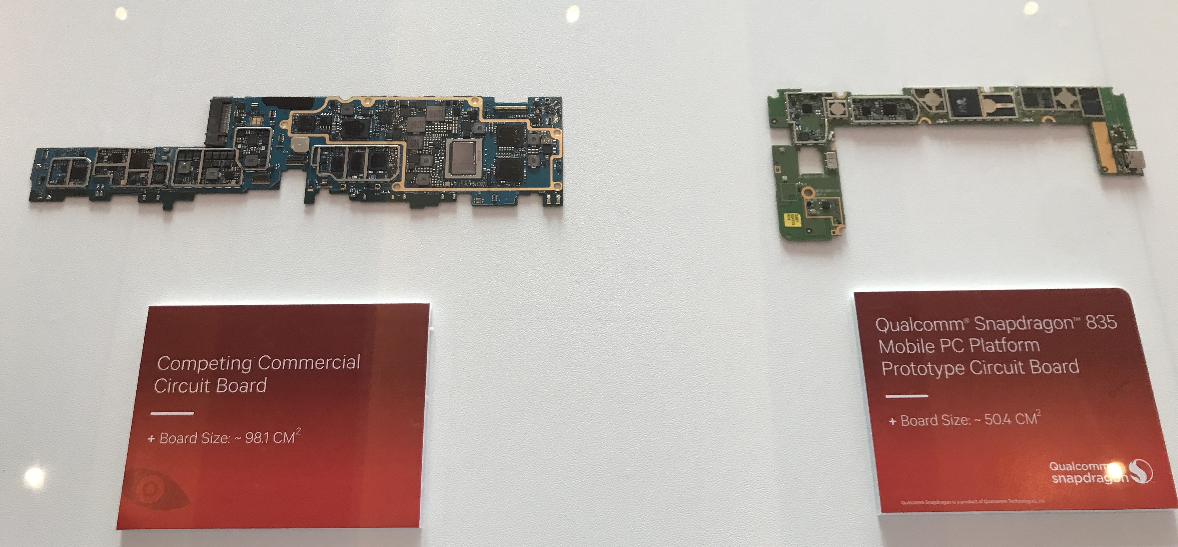
One of Qualcomm’s examples from 2018
For a Qualcomm processor designed for laptops, the silicon is a paired down to the essentials commonly associated with a smartphone. This means that modem connectivity is built into the processor, and the hardware associated with power delivery and USB are all on the scale of a smartphone. This means a motherboard designed around a Qualcomm processor will be around half the size, enabling different form factors, or more battery capacity in the same size laptop chassis.
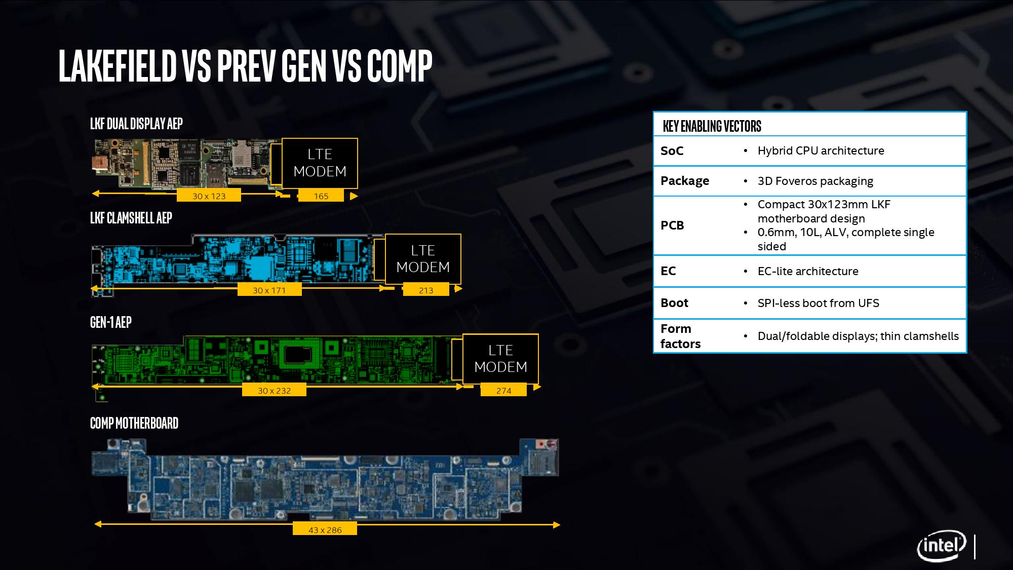
With Intel’s new Lakefield processor design, the chip is a lot smaller than previous Intel implementations. The company designed the processor from the ground up, with as much included on the CPU as to not need additional chips on the motherboard, and to fit the dimensions similar to one of Qualcomm’s processors. Above is a slide showing how Intel believes that with an LTE modem included, a Lakefield motherboard can move down to 7.7 square inches, similar to a Qualcomm design. This leaves more room for battery inside a device.
When Intel compares it against its own previous low power CPU implementations, the company quotes a 60% decrease in overall board area compared to its first generation 4.5 W processors.
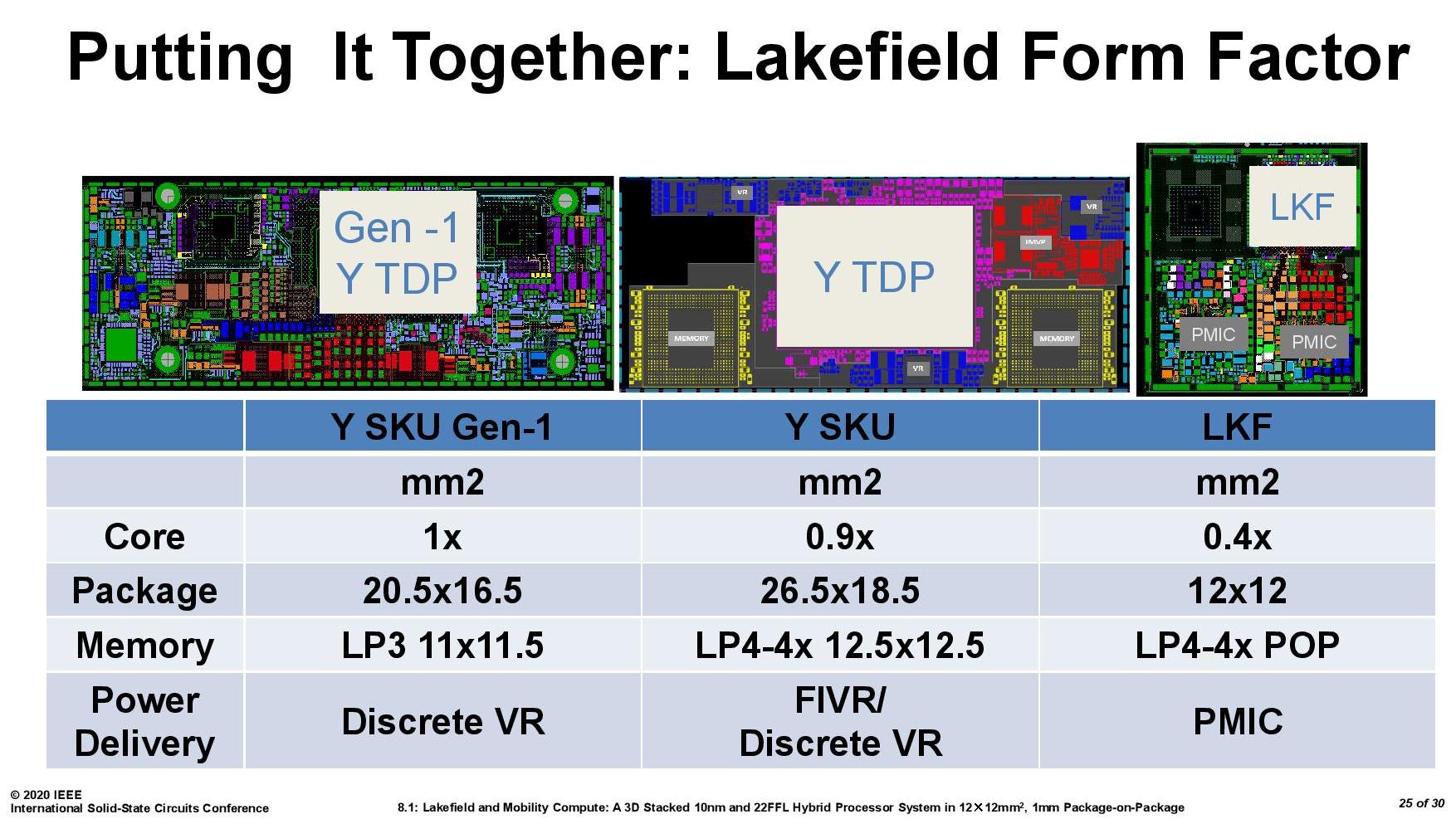
It is worth noting that for power delivery, Intel placed MIMCAPs inside the Lakefield silicon, much like a smartphone processor, and as a result it can get by on the power delivery implementation with a pair of PMICs (power management ICs). The reason why there is two is because of the two silicon dies inside – they are controlled differently for power for a number of technical reasons. If each layer within an active stacked implementation requires its own PMIC, that would presumably put an upper limit on future stacked designs – I fully expect Intel to be working on some sort of solution for this for it not to be an issue, however that wasn’t implemented in time for Lakefield.
For those that are interested, Lakefield’s PMICs are under the codenames Warren Cove and Castro Cover, and were developed in 2017-2018.


221 Comments
View All Comments
Drkrieger01 - Friday, July 3, 2020 - link
I'm not one to criticize, but this comment section is a dumpster fire.First of all, this is a FIRST GENERATION PRODUCT that hasn't even/barely made it to market.
Secondly, no one has really gotten to do a deep dive on performance of said product.
Thirdly, this processor package can be used from low end laptops, to tablets, and possibly it other mobile devices.
Fourth - who the hell cares about AVX? Do you people realize just how little AVX-512 is actually used in day-to-day usage scenarios that this CPU would be designed for? (mobile)
How about we wait to see what this product actually does for the technology market before we write it off as 'Intel Trash'.
/drops mic
Wilco1 - Friday, July 3, 2020 - link
What hasn't helped is that both Lakefield and Tremont have been hyped up for some time, so expectations were high. Some sites even claim that Tremont is a Cortex-A77 class core purely based on it having 2x3 decoders... That is setting things up for disappointment and failure."Wait for the next generation, it'll be great" has been used on every Atom, but it never lived up to its promise.
Deicidium369 - Sunday, July 5, 2020 - link
"Wait for the next generation, it'll be great" has been used on every AMD product, but it never lived up to its promise."Wilco1 - Sunday, July 5, 2020 - link
Without a doubt AMD has a much better track record than Intel - where are the 10nm desktops and servers? And Lakefield getting 60% of performance of the 18 month old 8cx is embarassing...lmcd - Sunday, July 5, 2020 - link
Track record is more than the last calendar year in a single market segment. You're kidding yourself if the company that brought Bulldozer, Piledriver, Steamroller, and Excavator to market promising that this was the one that fixed the architecture suddenly gets a pass on everything.Korguz - Monday, July 6, 2020 - link
and yet, it seems intel gets a pass when they make mistakes, or screw up. go figure.Spunjji - Monday, July 6, 2020 - link
Do you want to produce a similar list for the Pentium 4, Itanium, and Atom product ranges, or would that require a little too much intellectual honesty?Both companies have extended periods of bad products. Only one of them had the excuse of mediocre revenues, and only one of them was punished for their repeated failures with a dramatic loss in market share. Tells you a lot, really.
Spunjji - Monday, July 6, 2020 - link
Weird - pretty sure Athlon 64 was a rout, the first Athlon X2 was a rout, and Ryzen 3000 was a rout... You post some of the most asinine crap in this comment section when you're bagging on AMD, which is a real shame, because the rest of the time you seem to make a fair bit of sense.abufrejoval - Friday, July 3, 2020 - link
The entire article is about explaining what can already be inferred from the information we have at hand.Chips are engineering and physics, very little magic and a great degree of predictability.
None of the elements here are first generation, only their combination is a bit new. Ice Lake can be measured, you can benchmark a single core at 5 Watts with ThrottleStop and pinning the benchmark to a single core in any IceLake system. Atoms are well known and we can be sure that when Intel claims 23% improvement at the same power, it won't be 230%.
You can predict it's going to be much more expensive to make than a normal Atom, and you can measure that a single Core CPU below 5 Watts doesn't have a lot of horse power, while multiple cores on this design leave no Wattage for the big one.
This chip will be very expensive to make, so it won't sell at Atom prices. All the engineering is about making small enough to compete with ARM designs, yet capable of competing at 5Watts.
Yes, Ian could still be wrong here and there, but there isn't a lot of room to err.
The rest of us agree, that this chip will fail to make Intel rich and customers happy.
If we should be all wrong, remind us and we'll show proper contrition and learn.
But we bet on what we extrapolate from what we can know and measure, that's our duty as engineers.
lmcd - Sunday, July 5, 2020 - link
Tremont is absolutely new and the thermal characteristics of the package and layout also determine a lot.