The Intel Lakefield Deep Dive: Everything To Know About the First x86 Hybrid CPU
by Dr. Ian Cutress on July 2, 2020 9:00 AM ESTLakefield in Terms of Laptop Size
In a traditional AMD or Intel processor designed for laptops, we experience two to eight processing cores, along with some graphics performance, and it is up to the company to build the chip with the aim of hitting the right efficiency point (15 W, or 35/45 W) to enable the best performance for a given power window. These processors also contain a lot of extra connectivity and functionality, such as a dual channel memory controller, extra PCIe lanes to support external graphics, support for USB port connectivity or an external connectivity hub, or in the case of Intel’s latest designs, support for Thunderbolt built right into the silicon without the need for an external controller. These processors typically have physical dimensions of 150 square millimeters or more, and in a notebook, when paired with the additional power delivery and controllers needed such as Wi-Fi and modems, can tend towards the board inside the system (the motherboard) totaling 15 square inches total.
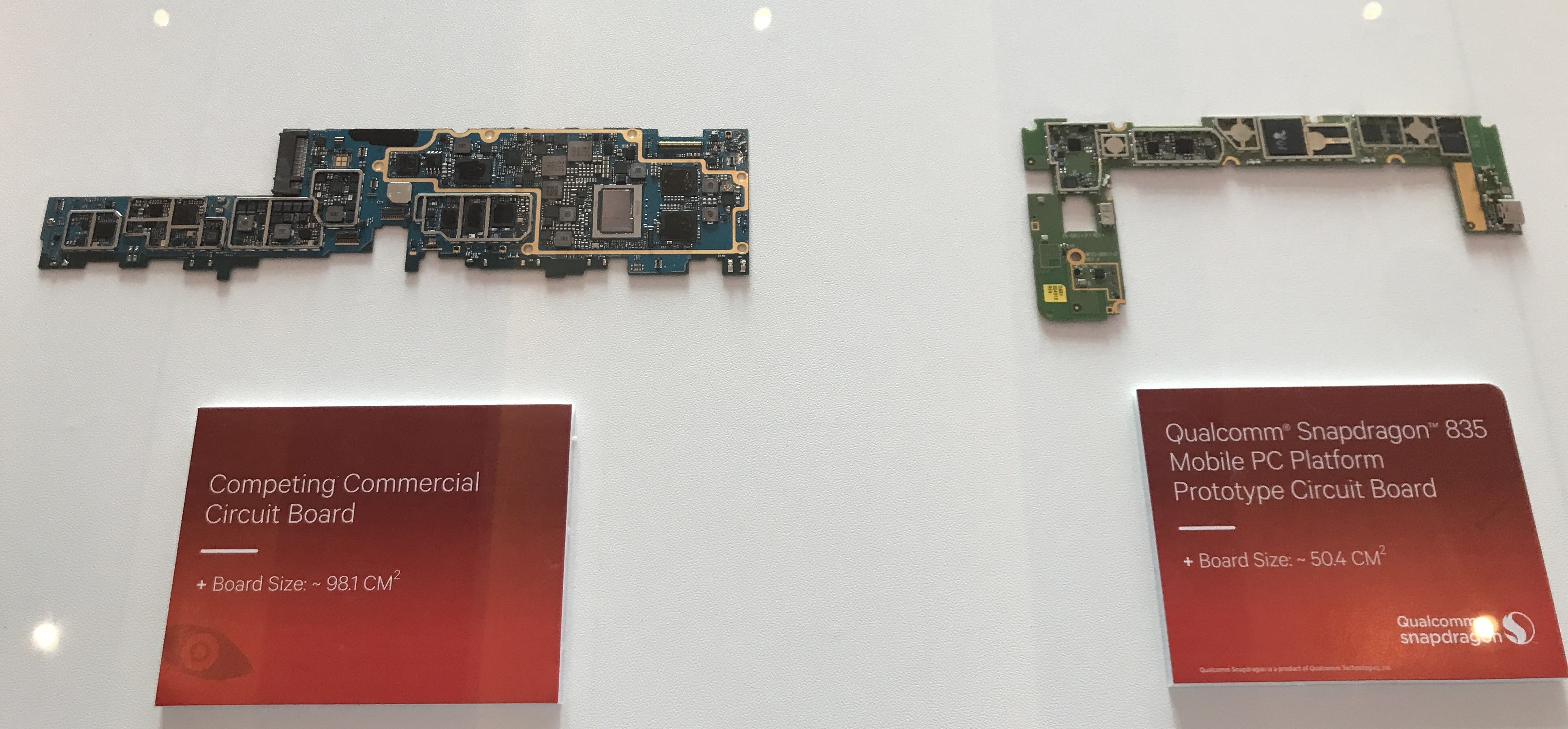
One of Qualcomm’s examples from 2018
For a Qualcomm processor designed for laptops, the silicon is a paired down to the essentials commonly associated with a smartphone. This means that modem connectivity is built into the processor, and the hardware associated with power delivery and USB are all on the scale of a smartphone. This means a motherboard designed around a Qualcomm processor will be around half the size, enabling different form factors, or more battery capacity in the same size laptop chassis.
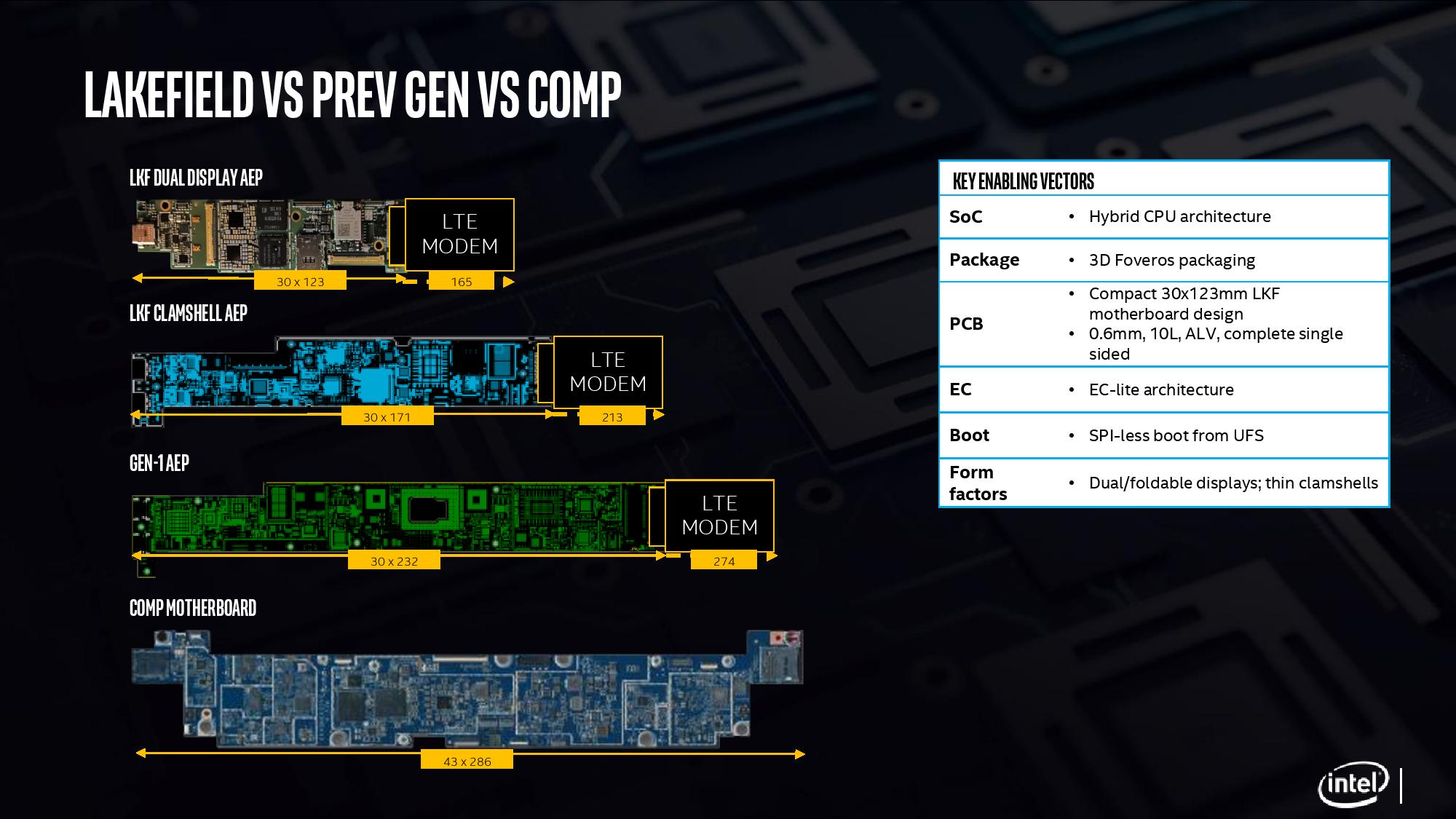
With Intel’s new Lakefield processor design, the chip is a lot smaller than previous Intel implementations. The company designed the processor from the ground up, with as much included on the CPU as to not need additional chips on the motherboard, and to fit the dimensions similar to one of Qualcomm’s processors. Above is a slide showing how Intel believes that with an LTE modem included, a Lakefield motherboard can move down to 7.7 square inches, similar to a Qualcomm design. This leaves more room for battery inside a device.
When Intel compares it against its own previous low power CPU implementations, the company quotes a 60% decrease in overall board area compared to its first generation 4.5 W processors.
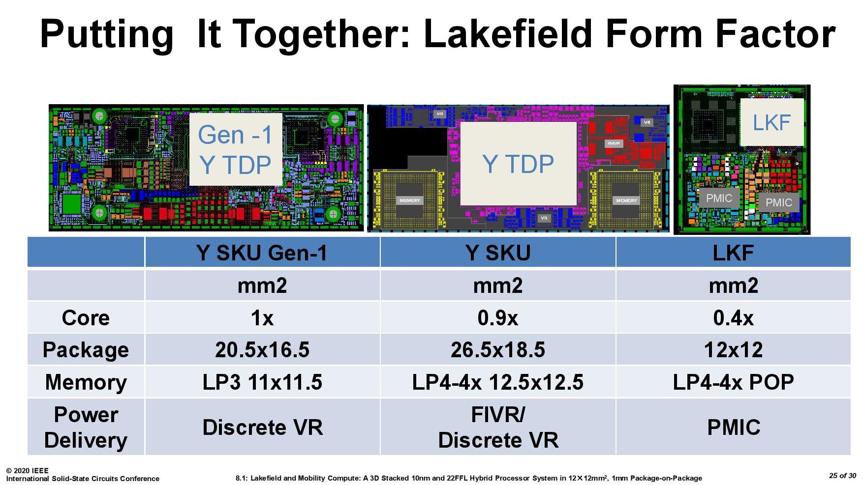
It is worth noting that for power delivery, Intel placed MIMCAPs inside the Lakefield silicon, much like a smartphone processor, and as a result it can get by on the power delivery implementation with a pair of PMICs (power management ICs). The reason why there is two is because of the two silicon dies inside – they are controlled differently for power for a number of technical reasons. If each layer within an active stacked implementation requires its own PMIC, that would presumably put an upper limit on future stacked designs – I fully expect Intel to be working on some sort of solution for this for it not to be an issue, however that wasn’t implemented in time for Lakefield.
For those that are interested, Lakefield’s PMICs are under the codenames Warren Cove and Castro Cover, and were developed in 2017-2018.


221 Comments
View All Comments
ichaya - Sunday, July 5, 2020 - link
The chart shows <10% power for <30% perf, and <20% power for <50% perf. That seems like 2-3x perf/watt difference as well. The A13 has a total of 28MB of cache shared between the CPU+GPU, where as this seems to have 6MB for the 4+1 CPU cores sans L1 caches.I'd love to see an Anandtech article on how Apple's large caches help with the code density differences between x86-64/ARM and with lower clock speeds, power consumption.
Wilco1 - Sunday, July 5, 2020 - link
The code density of AArch64 is significantly better than x86_64, so even at same cache sizes Arm has an advantage.ichaya - Wednesday, July 8, 2020 - link
Source? Everything I've read says x86-64 still has a diminishing but slight advantage in code density. If anything, lower clock speeds are helping Apple by avoiding memory pressure issues at higher clock speeds. I highly doubt AArch64 could perform the same as x86-64 with equal caches at any clock speed. uArch differences could outweigh these differences, but I've seen evidence of this given how large Apple's caches have been.ichaya - Wednesday, July 8, 2020 - link
* I've seen no evidence of this given how large Apple's caches have been.Correcting the last sentence in post above.
Wilco1 - Wednesday, July 8, 2020 - link
No, x86 has never had good code density, 32-bit x86 is terrible compared to Thumb-2. x86_64 has worse code density than 32-bit x86, and it gets really bad if you use SIMD instructions.Try building a large binary on both systems using the same compiler and compare the .text sizes. For example I use all of SPEC2017 built with identical GCC version and options. AArch64 code is generally 10-15% smaller.
Many AArch64 cores already have higher IPC - yes that absolutely means they are faster than x86 cores at the same clock frequency using similar sized caches.
This https://images.anandtech.com/graphs/graph15578/115... shows Neoverse N1 has ~28% higher IPC than EPYC 7571 and ~21% higher IPC than Xeon Platinum 8259 on SPECINT2017. While Naples has 2x8MB LLC on each chiplet, the Xeon has 36MBytes, more than the 32MB in Graviton 2 (both also have 1MB L2 per core).
Recent cores like Cortex-A78 and Cortex-X1 are 30-50% faster than Neovere N1. Do the math and see where this is going. 2020 is the year when AArch64 servers outperform the fastest x86 servers, 2021 may be the year when AArch64 CPUs outperform the fastest x86 desktops.
ichaya - Saturday, July 11, 2020 - link
If you compare with -march=x86-64 or with a specific uArch like -march=haswell you'll get comparable code sizes to -march=armv8.4-a. But form the runtime code density differences I've seen, x86-64 still seems to have a slight advantage.From the article you linked the image from (https://www.anandtech.com/show/15578/cloud-clash-a... "If we were to divide the available cache on a per-thread basis, the Graviton2 leads the set at 1.5MB, ahead of the EPYC’s 1.25MB and the Xeon’s 1.05MB." ARM's system-level cache is good idea, as is shared L2 in Apple's A* chips. But cache advantages per thread in Graviton and A* seem to signal it's not the uArch making the difference. Similar cores to Graviton's cores with less cache, do a lot worse. Not being able to clock higher than 2.5Ghz also seems to signal that the uArch/interconnects cannot keep up with memory pressure.
To the extent that die sizes of these chips (Graviton 2 is 7nm, Epyc 7571 and Intel Xeon 8259CL are 14nm) are comparable, it's features like AVX2/SMT that seem to have been replaced with cache in the benchmarks in the article. I'll be looking forward to A* chips to see how they might stack up in Laptops and Desktops, but these are the doubts I still have.
ichaya - Saturday, July 11, 2020 - link
Correct link in post above: https://www.anandtech.com/show/15578/cloud-clash-a...Wilco1 - Saturday, July 11, 2020 - link
Runtime code density? Do you mean accurately counting total bytes fetched from L1I and MOP cache? x86 won't look good because of the inefficiency of byte-aligned instructions, needing 2 extra predecode bits per byte and MOPs being very wide on x86 (64 bits in SandyBridge)... It clearly shows why byte-sized instructions are a bad idea.The graph I posted is for single-threaded performance, so the amount of cache per-thread is not relevant at all. Arm's IPC is higher and thus it is a better micro architecture than Skylake and EPYC 1. IPC is also ~12% better than EPYC 7742 based on https://www.anandtech.com/show/14694/amd-rome-epyc...
In terms of all-core throughput the fastest EPYC 7742 does only ~30% better than Graviton 2 on INTrate2006. That's pretty awful considering it has 8 times the L3 cache (yes eight times!!!), twice the threads, runs at up to 3.4GHz and uses twice the power...
In terms of die size, EPYC 7742 is ~3 times larger in 7nm, so it's extremely area inefficient compared to Graviton 2. So any suggestion that cache is used to make a weak core look better should surely be directed at EPYC?
Graviton 2 is a very conservative design to save cost, hence the low 2.5GHz frequency. Ampere Altra pushes the limits with 80 Neoverse N1 cores at 3.3GHz base (yes that's base, not turbo!). Next year it will have 128 cores, competing with 128 threads in EPYC 3. Guess how that will turn out?
ichaya - Sunday, July 12, 2020 - link
Code density and decoding instructions are separate things. Here's an older paper on code density of a particular program: http://web.eece.maine.edu/~vweaver/papers/iccd09/l...Single threaded workloads are obviously going to do better with a shared system-level and in Apple's case, shared L2 caches. Sharing caches is something that Intel is closer to than AMD. You cannot compare INTrate2006 or any single threaded benchmark running on an ARM where all system-level caches are available for one thread with an Epyc 7742 where only 1 CCX's L3 caches are available to one thread. That would be 32MB on Graviton 2 vs 16MB on an AMD EPYC 2 CCX. So, AMD is being 30% faster with 1/2 the cache and clocked 30% higher than Graviton 2.
I will definitely give credit to efficient shared system/L2 cache usage to Graviton 2, A*, and other ARM chips, but comparing power usage when there are 64 cores of AVX2 on chip when there's nothing comparable on another is an irrelevant comparison if there ever was one.
Wilco1 - Sunday, July 12, 2020 - link
The complexity and overhead of instruction decoding is closely related with the ISA. Byte-aligned instructions have a large cost, and since they don't give a code density advantage, it's an even larger cost! Again if you want to study code density, compare all of SPEC or a whole Linux distro. Code density of huge amounts of compiled code is what matters in the real world, not tiny examples that are a few hundred bytes!Well EPYC 7742 is only 21% faster single threaded while being clocked 36% faster. Sure Graviton 2 has twice the L3 available, but the difference between 16 and 32MBytes is hardly going to be 12%. If every doubling gave 10% then the easiest way to improve performance was to keep doubling caches!
AVX isn't used much, surely not in SPEC, so it contributes little to total power consumption (unless you're trying to say that x86 designers are totally incompetent?). At the end of the day getting good perf/W matters to data centers, not whether a core has AVX or not.