The Intel Lakefield Deep Dive: Everything To Know About the First x86 Hybrid CPU
by Dr. Ian Cutress on July 2, 2020 9:00 AM ESTThermal Management on Stacked Silicon
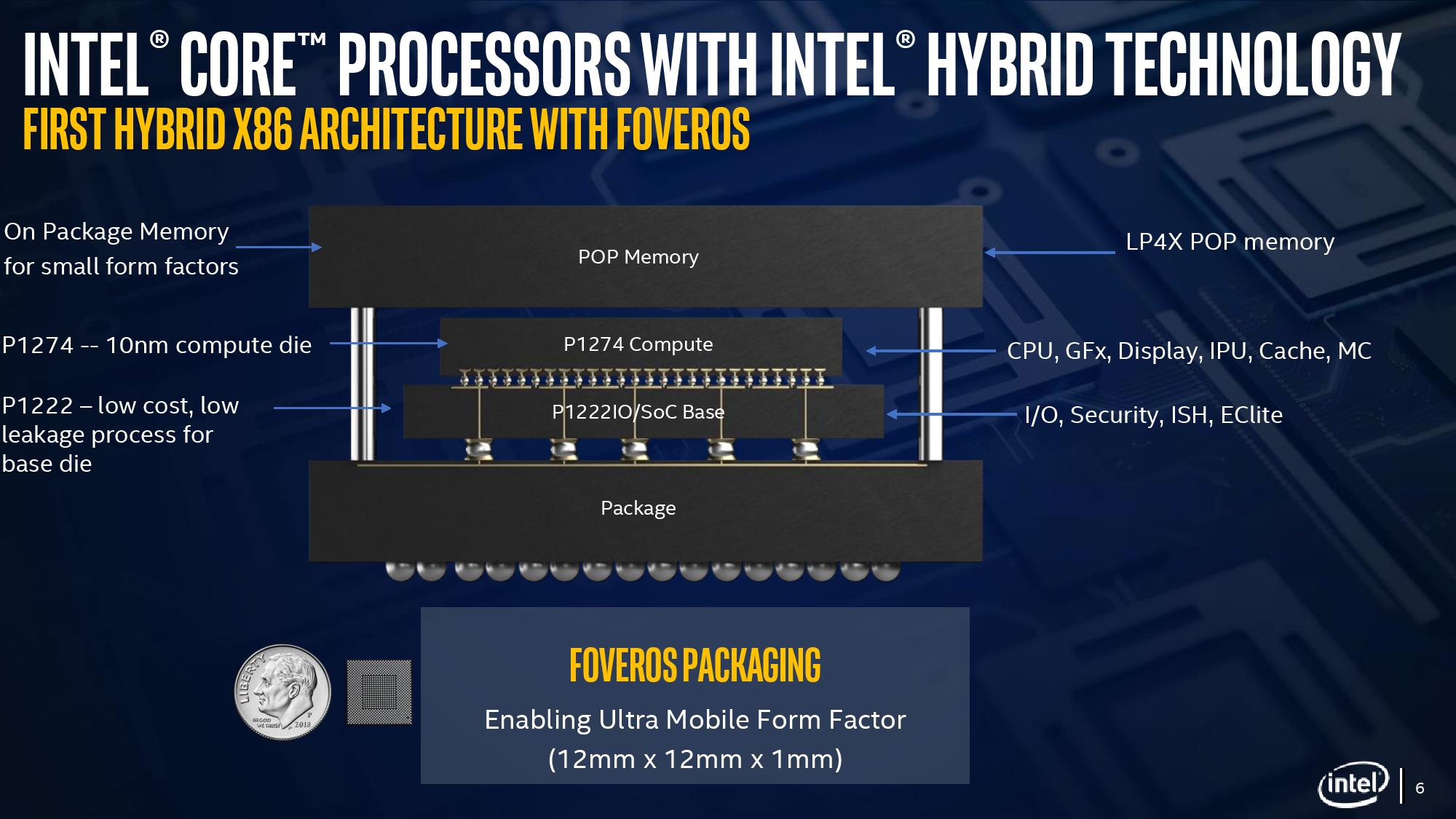
With a standard processor design, there is a single piece of silicon doing all the work and generating the heat – it’s bonded to the package (which doesn’t do any work) and then depending on the implementation, there’s some adhesive to either a cooler or a headspreader then a cooler. When moving to a stacked chiplet design, it gets a bit more complicated.
Having two bits of silicon that ‘do work’, even if one is the heavy compute die and the other is an active interposer taking care of USB and audio and things, does mean that there’s a thermal gradient between the silicon, and depending on the bonding, potential for thermal hotspots and build-up. Lakefield makes it even more complex, by having an additional DRAM package placed on top but not directly bonded.
We can take each of these issues independently. For the case of die-on-die interaction, there is a lot of research going into this area. Discussions and development about fluidic channels between two hot silicon dies have been going on for a decade or longer in academia, and Intel has mentioned it a number of times, especially when relating to a potential solution of its new die-to-die stacking technology.
They key here is hot dies, with thermal hotspots. As with a standard silicon design, ideally it is best to keep two high-powered areas separate, as it gives a number of benefits with power delivery, cooling, and signal integrity. With a stacked die, it is best to not have hotspots directly on top of each other, for similar reasons. Despite Intel using its leading edge 10+ process node for the compute die, the base die is using 22FFL, which is Intel’s low power implementation of its 14nm process. Not only that, but the base die is only dealing with IO, such as USB and PCIe 3.0, which is essentially fixed bandwidth and energy costs. What we have here is a high-powered die on top of a low powered die, and as such thermal issues between the two silicon die, especially in a low TDP device like Lakefield (7W TDP), are not an issue.
What is an issue is how the compute die gets rid of the heat. On the bottom it can do convection by being bonded to more silicon, but the top is ultimately blocked by that DRAM die. As you can see in the image above, there’s a big air gap between the two.
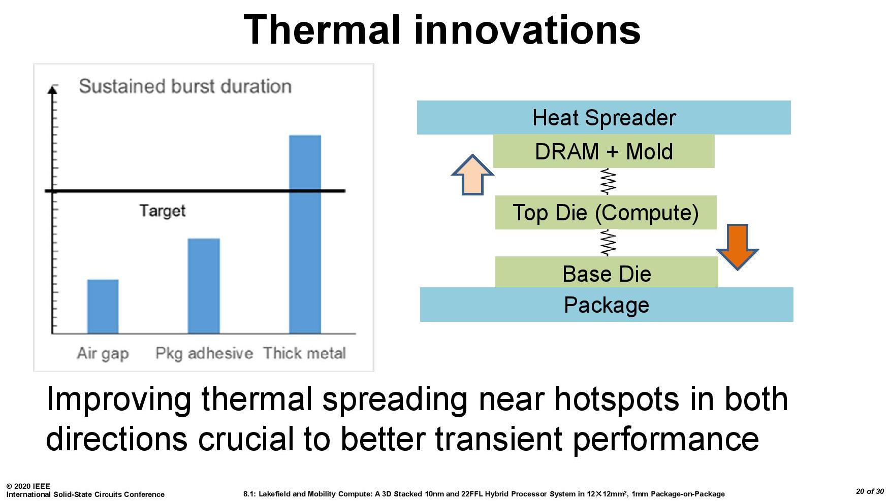
As part of the Lakefield design, Intel had to add in a number of design changes in order to make the thermals work. A lot of work can be done with the silicon design itself, such as matching up hotspots in the right area, using suitable thickness of metals in various layers, and rearranging the floorplan to reduce localized power density. Ultimately both increasing the thermal mass and the potential dissipation becomes high priorities.
Lakefield CPUs have a sustained power limit of 7 watts – this is defined in the specifications. Intel also has another limit, known as the turbo power limit. At Intel’s Architecture Day, the company stated that the turbo power limit was 27 watts, however in the recent product briefing, we were told is set at 9.5 W. Historically Intel will let its OEM partners (Samsung, Lenovo, Microsoft) choose its own values for these based on how well the design implements its cooling – passive vs active and heatsink mass and things like this. Intel also has another factor of turbo time, essentially a measure of how long the turbo power can be sustained for.
When we initially asked Intel for this value, they refused to tell us, stating that it is proprietary information. After I asked again after a group call on the product, I got the same answer, despite the fact that I informed the Lakefield team that Intel has historically given this information out. Later on, I found out through my European peers that in a separate briefing, they gave the value of 28 seconds, to which Intel emailed me this several hours afterwards. This value can also be set by OEMs.
Then I subsequently found one of Intel’s ISSCC slides.
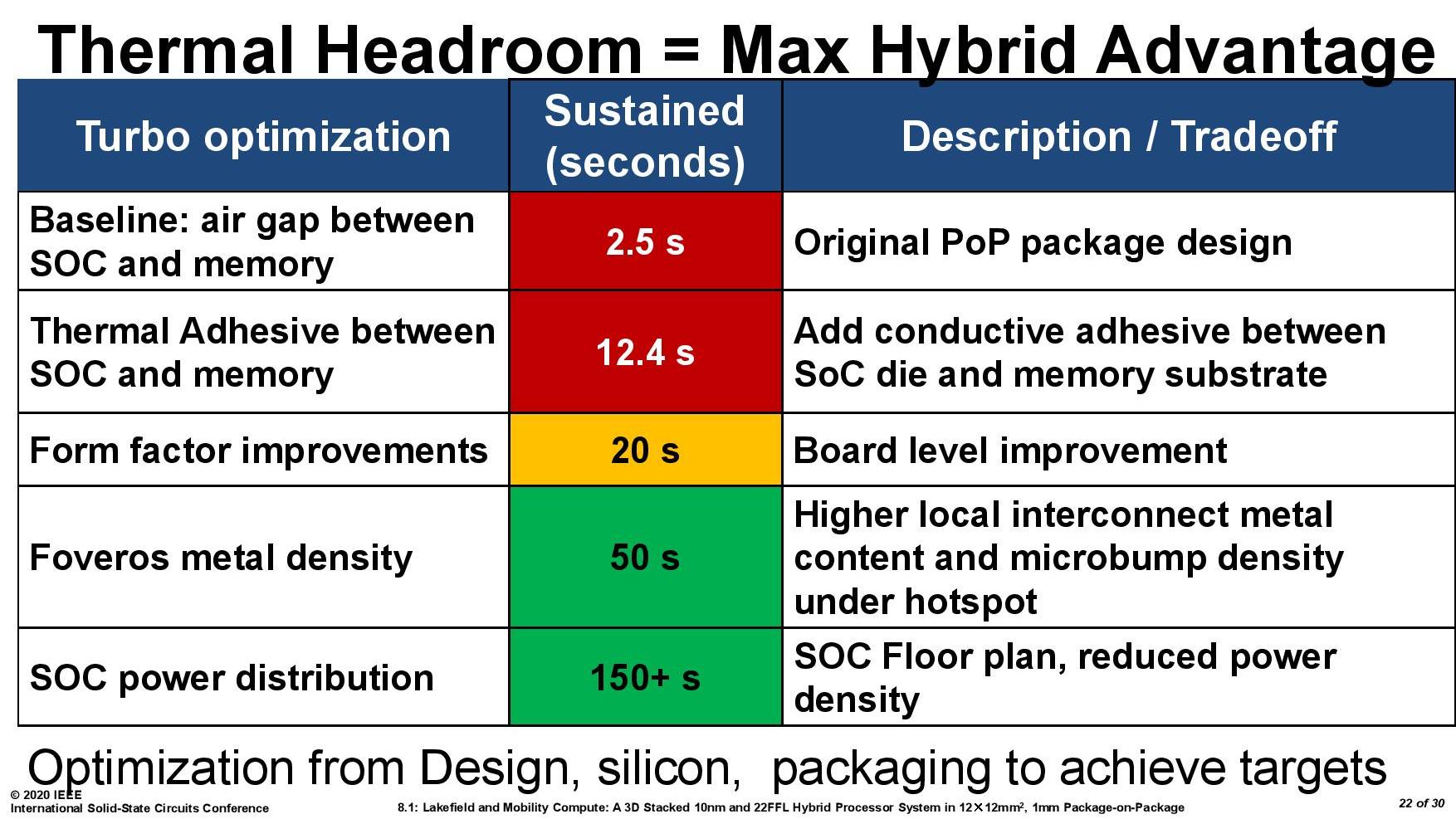
This slide shows that a basic implementation would only allow sustained power for 2.5 seconds. Adding in an adhesive between the top die and the DRAM moves up to 12.4 seconds, and then improving the system cooling goes up to 20 seconds. The rest of the improvements work below the compute die: a sizeable improvement comes from increasing the die-to-die metal density, and then an optimized power floor plan which in total gives sustained power support for 150+ seconds.


221 Comments
View All Comments
ichaya - Sunday, July 5, 2020 - link
The chart shows <10% power for <30% perf, and <20% power for <50% perf. That seems like 2-3x perf/watt difference as well. The A13 has a total of 28MB of cache shared between the CPU+GPU, where as this seems to have 6MB for the 4+1 CPU cores sans L1 caches.I'd love to see an Anandtech article on how Apple's large caches help with the code density differences between x86-64/ARM and with lower clock speeds, power consumption.
Wilco1 - Sunday, July 5, 2020 - link
The code density of AArch64 is significantly better than x86_64, so even at same cache sizes Arm has an advantage.ichaya - Wednesday, July 8, 2020 - link
Source? Everything I've read says x86-64 still has a diminishing but slight advantage in code density. If anything, lower clock speeds are helping Apple by avoiding memory pressure issues at higher clock speeds. I highly doubt AArch64 could perform the same as x86-64 with equal caches at any clock speed. uArch differences could outweigh these differences, but I've seen evidence of this given how large Apple's caches have been.ichaya - Wednesday, July 8, 2020 - link
* I've seen no evidence of this given how large Apple's caches have been.Correcting the last sentence in post above.
Wilco1 - Wednesday, July 8, 2020 - link
No, x86 has never had good code density, 32-bit x86 is terrible compared to Thumb-2. x86_64 has worse code density than 32-bit x86, and it gets really bad if you use SIMD instructions.Try building a large binary on both systems using the same compiler and compare the .text sizes. For example I use all of SPEC2017 built with identical GCC version and options. AArch64 code is generally 10-15% smaller.
Many AArch64 cores already have higher IPC - yes that absolutely means they are faster than x86 cores at the same clock frequency using similar sized caches.
This https://images.anandtech.com/graphs/graph15578/115... shows Neoverse N1 has ~28% higher IPC than EPYC 7571 and ~21% higher IPC than Xeon Platinum 8259 on SPECINT2017. While Naples has 2x8MB LLC on each chiplet, the Xeon has 36MBytes, more than the 32MB in Graviton 2 (both also have 1MB L2 per core).
Recent cores like Cortex-A78 and Cortex-X1 are 30-50% faster than Neovere N1. Do the math and see where this is going. 2020 is the year when AArch64 servers outperform the fastest x86 servers, 2021 may be the year when AArch64 CPUs outperform the fastest x86 desktops.
ichaya - Saturday, July 11, 2020 - link
If you compare with -march=x86-64 or with a specific uArch like -march=haswell you'll get comparable code sizes to -march=armv8.4-a. But form the runtime code density differences I've seen, x86-64 still seems to have a slight advantage.From the article you linked the image from (https://www.anandtech.com/show/15578/cloud-clash-a... "If we were to divide the available cache on a per-thread basis, the Graviton2 leads the set at 1.5MB, ahead of the EPYC’s 1.25MB and the Xeon’s 1.05MB." ARM's system-level cache is good idea, as is shared L2 in Apple's A* chips. But cache advantages per thread in Graviton and A* seem to signal it's not the uArch making the difference. Similar cores to Graviton's cores with less cache, do a lot worse. Not being able to clock higher than 2.5Ghz also seems to signal that the uArch/interconnects cannot keep up with memory pressure.
To the extent that die sizes of these chips (Graviton 2 is 7nm, Epyc 7571 and Intel Xeon 8259CL are 14nm) are comparable, it's features like AVX2/SMT that seem to have been replaced with cache in the benchmarks in the article. I'll be looking forward to A* chips to see how they might stack up in Laptops and Desktops, but these are the doubts I still have.
ichaya - Saturday, July 11, 2020 - link
Correct link in post above: https://www.anandtech.com/show/15578/cloud-clash-a...Wilco1 - Saturday, July 11, 2020 - link
Runtime code density? Do you mean accurately counting total bytes fetched from L1I and MOP cache? x86 won't look good because of the inefficiency of byte-aligned instructions, needing 2 extra predecode bits per byte and MOPs being very wide on x86 (64 bits in SandyBridge)... It clearly shows why byte-sized instructions are a bad idea.The graph I posted is for single-threaded performance, so the amount of cache per-thread is not relevant at all. Arm's IPC is higher and thus it is a better micro architecture than Skylake and EPYC 1. IPC is also ~12% better than EPYC 7742 based on https://www.anandtech.com/show/14694/amd-rome-epyc...
In terms of all-core throughput the fastest EPYC 7742 does only ~30% better than Graviton 2 on INTrate2006. That's pretty awful considering it has 8 times the L3 cache (yes eight times!!!), twice the threads, runs at up to 3.4GHz and uses twice the power...
In terms of die size, EPYC 7742 is ~3 times larger in 7nm, so it's extremely area inefficient compared to Graviton 2. So any suggestion that cache is used to make a weak core look better should surely be directed at EPYC?
Graviton 2 is a very conservative design to save cost, hence the low 2.5GHz frequency. Ampere Altra pushes the limits with 80 Neoverse N1 cores at 3.3GHz base (yes that's base, not turbo!). Next year it will have 128 cores, competing with 128 threads in EPYC 3. Guess how that will turn out?
ichaya - Sunday, July 12, 2020 - link
Code density and decoding instructions are separate things. Here's an older paper on code density of a particular program: http://web.eece.maine.edu/~vweaver/papers/iccd09/l...Single threaded workloads are obviously going to do better with a shared system-level and in Apple's case, shared L2 caches. Sharing caches is something that Intel is closer to than AMD. You cannot compare INTrate2006 or any single threaded benchmark running on an ARM where all system-level caches are available for one thread with an Epyc 7742 where only 1 CCX's L3 caches are available to one thread. That would be 32MB on Graviton 2 vs 16MB on an AMD EPYC 2 CCX. So, AMD is being 30% faster with 1/2 the cache and clocked 30% higher than Graviton 2.
I will definitely give credit to efficient shared system/L2 cache usage to Graviton 2, A*, and other ARM chips, but comparing power usage when there are 64 cores of AVX2 on chip when there's nothing comparable on another is an irrelevant comparison if there ever was one.
Wilco1 - Sunday, July 12, 2020 - link
The complexity and overhead of instruction decoding is closely related with the ISA. Byte-aligned instructions have a large cost, and since they don't give a code density advantage, it's an even larger cost! Again if you want to study code density, compare all of SPEC or a whole Linux distro. Code density of huge amounts of compiled code is what matters in the real world, not tiny examples that are a few hundred bytes!Well EPYC 7742 is only 21% faster single threaded while being clocked 36% faster. Sure Graviton 2 has twice the L3 available, but the difference between 16 and 32MBytes is hardly going to be 12%. If every doubling gave 10% then the easiest way to improve performance was to keep doubling caches!
AVX isn't used much, surely not in SPEC, so it contributes little to total power consumption (unless you're trying to say that x86 designers are totally incompetent?). At the end of the day getting good perf/W matters to data centers, not whether a core has AVX or not.