The Intel Lakefield Deep Dive: Everything To Know About the First x86 Hybrid CPU
by Dr. Ian Cutress on July 2, 2020 9:00 AM ESTLakefield in Terms of Laptop Size
In a traditional AMD or Intel processor designed for laptops, we experience two to eight processing cores, along with some graphics performance, and it is up to the company to build the chip with the aim of hitting the right efficiency point (15 W, or 35/45 W) to enable the best performance for a given power window. These processors also contain a lot of extra connectivity and functionality, such as a dual channel memory controller, extra PCIe lanes to support external graphics, support for USB port connectivity or an external connectivity hub, or in the case of Intel’s latest designs, support for Thunderbolt built right into the silicon without the need for an external controller. These processors typically have physical dimensions of 150 square millimeters or more, and in a notebook, when paired with the additional power delivery and controllers needed such as Wi-Fi and modems, can tend towards the board inside the system (the motherboard) totaling 15 square inches total.
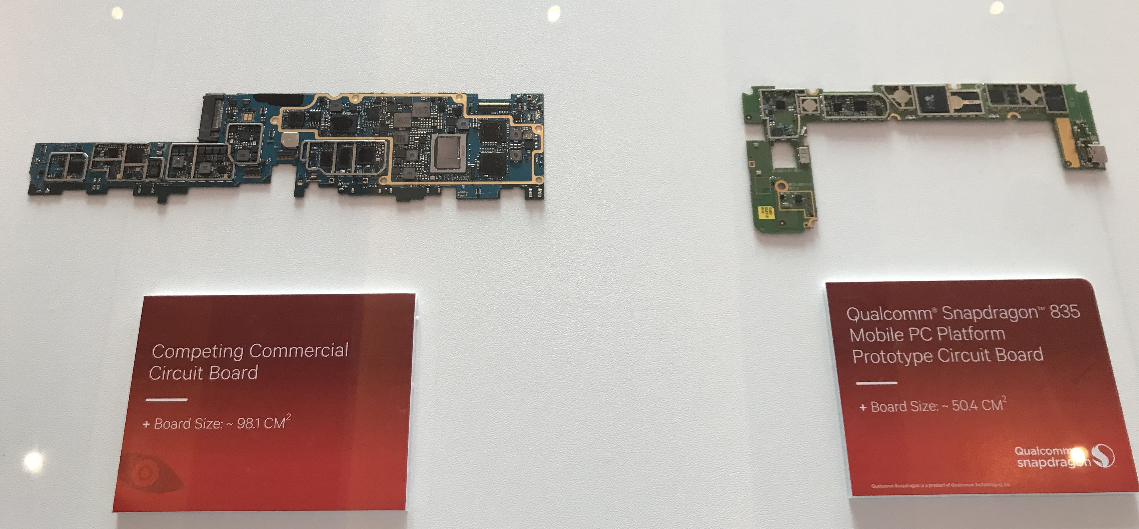
One of Qualcomm’s examples from 2018
For a Qualcomm processor designed for laptops, the silicon is a paired down to the essentials commonly associated with a smartphone. This means that modem connectivity is built into the processor, and the hardware associated with power delivery and USB are all on the scale of a smartphone. This means a motherboard designed around a Qualcomm processor will be around half the size, enabling different form factors, or more battery capacity in the same size laptop chassis.
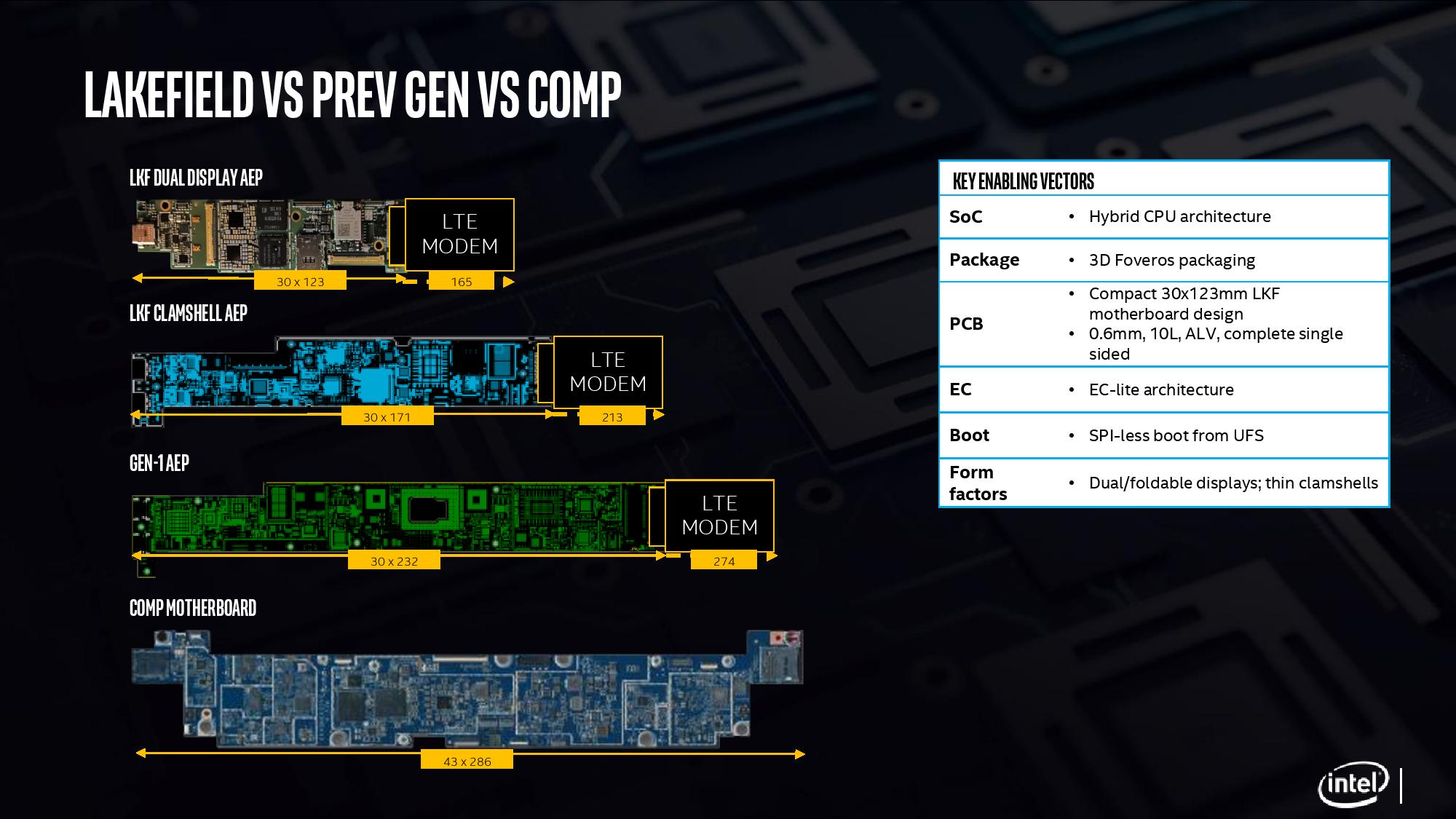
With Intel’s new Lakefield processor design, the chip is a lot smaller than previous Intel implementations. The company designed the processor from the ground up, with as much included on the CPU as to not need additional chips on the motherboard, and to fit the dimensions similar to one of Qualcomm’s processors. Above is a slide showing how Intel believes that with an LTE modem included, a Lakefield motherboard can move down to 7.7 square inches, similar to a Qualcomm design. This leaves more room for battery inside a device.
When Intel compares it against its own previous low power CPU implementations, the company quotes a 60% decrease in overall board area compared to its first generation 4.5 W processors.
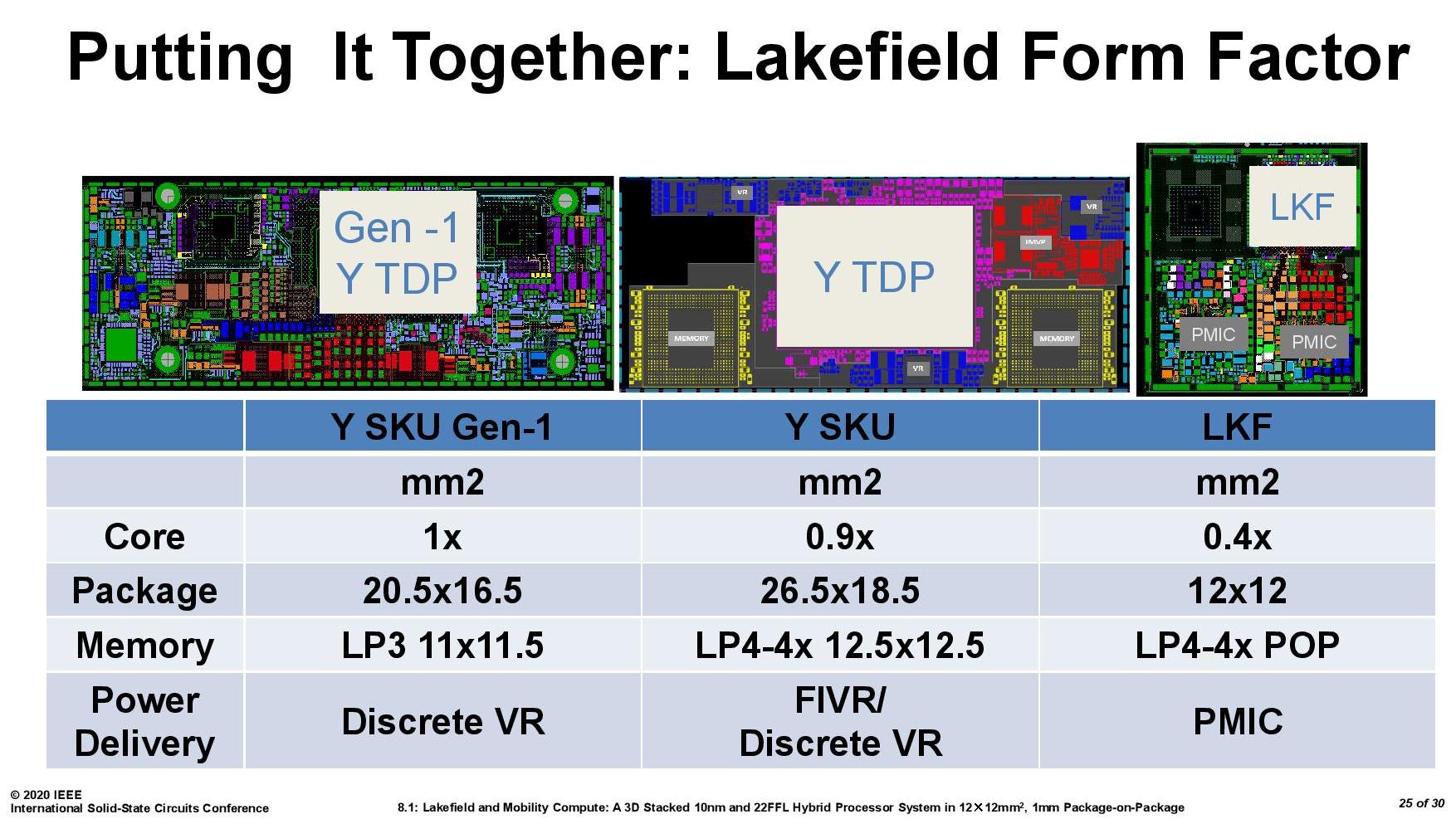
It is worth noting that for power delivery, Intel placed MIMCAPs inside the Lakefield silicon, much like a smartphone processor, and as a result it can get by on the power delivery implementation with a pair of PMICs (power management ICs). The reason why there is two is because of the two silicon dies inside – they are controlled differently for power for a number of technical reasons. If each layer within an active stacked implementation requires its own PMIC, that would presumably put an upper limit on future stacked designs – I fully expect Intel to be working on some sort of solution for this for it not to be an issue, however that wasn’t implemented in time for Lakefield.
For those that are interested, Lakefield’s PMICs are under the codenames Warren Cove and Castro Cover, and were developed in 2017-2018.


221 Comments
View All Comments
Spunjji - Monday, July 6, 2020 - link
Given the cost of producing multiple dies, stacking them, and packaging the whole lot with RAM on top - I doubt even that's going to be particularly compelling. It probably would have been better if they'd transitioned fully to 10nm and had idle 14nm capacity, but as it stands this will be competing for manufacturing space with their own premium products on both lines. D:lmcd - Friday, July 3, 2020 - link
This isn't designed for Windows. This is designed for Windows 10X. Windows 10X got delayed so partners are shipping it with Windows.serendip - Friday, July 3, 2020 - link
Will Win10X bring a magical doubling in performance?Spunjji - Monday, July 6, 2020 - link
My thoughts exactly. I feel like they've tried to do too many things at the same time with this product.They obviously wanted to demonstrate Foveros with a relatively low-complexity, relatively low-power chip - but the cost of the first-gen Foveros tech conflicts with one of the big primary selling points of small chips in the first place, i.e. lower cost. So they've gone for a "premium" product, but the first-gen Foveros tech puts a fairly low ceiling on its performance - meaning it's not actually very premium in practice.
It's a quagmire of mutually contradictory requirements, and tbh that's pretty on-par with Intel's previous efforts in the low-power CPU arena.
lmcd - Thursday, July 2, 2020 - link
Honestly confused why everyone is up in arms about the lack of AVX. This is a tablet SoC for Windows 10X and any other usage of it is outside of its intended scope. Future SoCs might add more of this functionality but it doesn't really seem like a priority. A low-power SoC that also won't wilt to the render thread and "just works" with legacy x86-only apps when necessary sounds good to me.Spunjji - Monday, July 6, 2020 - link
I think it's mainly that Intel have spent so much time selling that feature so hard, then dropped it - albeit without actually physically removing it. So, once again, Intel are charging their customers money to manufacture something in silicon that they can't actually use.xdrol - Thursday, July 2, 2020 - link
The Snapdragon 7c is more like a 2+6 than a 0+8 chip: It has 2x Kryo Gold (Cortex A76) and 6x Kryo Silver (A55) cores.Sychonut - Friday, July 3, 2020 - link
I am not sure I understand whether the added design complexity is justified by the very minor power savings as depicted by the power / performance graph on page 1, or am I reading it wrong? The difference between the two curves seems marginal at best below 58%.ichaya - Friday, July 3, 2020 - link
That seems like the most meaningful part of the chart. You can still deliver 60%+ performance with only 30-50% of the power.This is a 1st gen attempt and a 2+4 design with AVX and ARM's System-level cache would definitely be interesting to see in ultra portables.
unclevagz - Friday, July 3, 2020 - link
Which itself is not a good showing for the 'efficiency' core, the small thunder cores in the Apple A13 are at ~20-30% of the Lightning core's performance while consuming 5-15% of the power (2-3x perf/watt) . And the A13 Lightning in all likelihood already runs rings around the lakefield cores in this department.