Intel at Hot Chips 2018: Showing the Ankle of Cascade Lake
by Ian Cutress on August 19, 2018 7:30 PM EST- Posted in
- CPUs
- Intel
- Spectre
- AVX-512
- Meltdown
- Cascade Lake
- Optane DIMMs
- VNNI
Purley Mark Two: Cascade Lake-SP
On the processor front, the on-paper hardware specifications of Cascade Lake Xeons offer no surprises, mainly because the stock design is identical to Skylake Xeons. Users will be offered up to 28 cores with hyperthreading, the same levels of cache, the same UPI connectivity, the same number of PCIe lanes, the same number of channels of memory, and the same maximum supported frequency of memory.
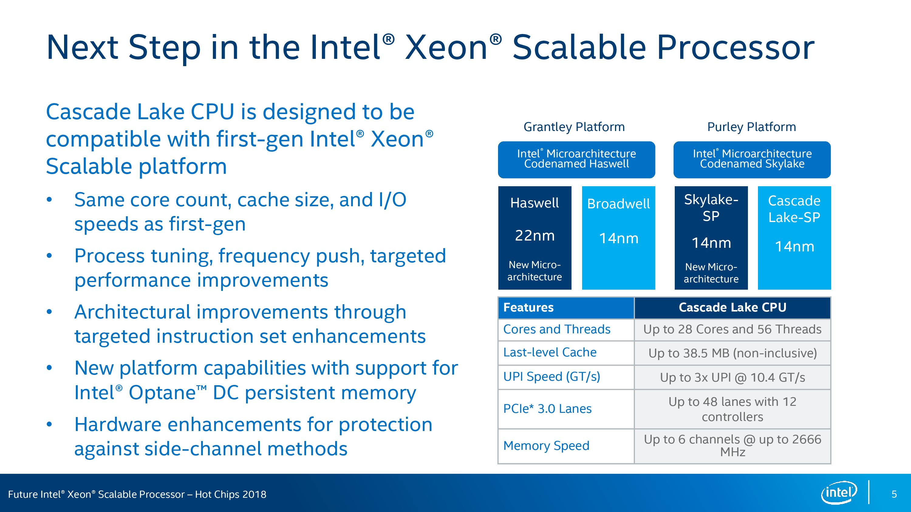
Questions still to be answered will be if the XCC/HCC/LCC silicon dies, from which the processor stack will come, will be the same. There is also no information about memory capacity limitations.
What Intel is saying on this slide however is in the second bullet point:
- Process tuning, frequency push, targeted performance improvements
We believe this is a tie-in to Intel improving its 14nm process further, tuning it for voltage and frequency, or a better binning. At this point Intel has not stated if Cascade Lake is using the ‘14++’ process node, to use Intel’s own naming scheme, although we expect it to be the case. We suspect that Intel might drop the +++ naming scheme altogether, if this isn’t disclosed closer to the time. However a drive to 10% better frequency at the same voltage would be warmly welcomed.
Where some of the performance will come from is in the new deep learning instructions, as well as the support for Optane DIMMs.
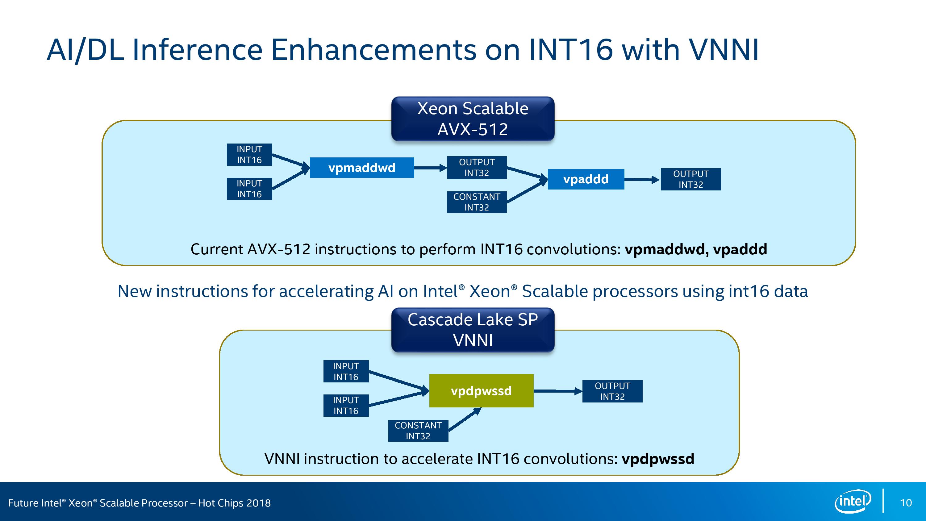
AVX-512 VNNI Instructions for Deep Learning
The world of AVX-512 instruction support is completely confusing. Different processors and different families support various sets of instructions, and it is hard to keep track of them all, let alone code for them. Luckily for Intel (and others), companies that invest into deep learning tend to focus on one particular set of microarchitectures for their work. As a result, Intel has been working with software developers to optimize code paths for Xeon Scalable systems. In fact, Intel is claiming to have already secured a 5.4x increase in inference throughput on Caffe / ResNet50 since the launch of Skylake – partially though code and parallelism optimizations, but partially though reduced precision and multiple concurrent instances also.
With VNNI, or Vector Neural Network Instructions, Intel expects to double its neural network performance with Cascade Lake. Behind VNNI are two key instructions that can optimized and decoded, reducing work:

Both instructions aim to reduce the number of required manipulations within inner convulsion loops for neural networks.
VPDPWSSD, the INT16 version of the two instructions, fuses two INT16 instructions and uses a third INT32 constant to replace PMADDWD and VPADD math that current AVX-512 would use:
VPDPBUSD does a similar thing, but takes it one stage back, using INT8 inputs to reduce a three-instruction path into a one-instruction implementation:
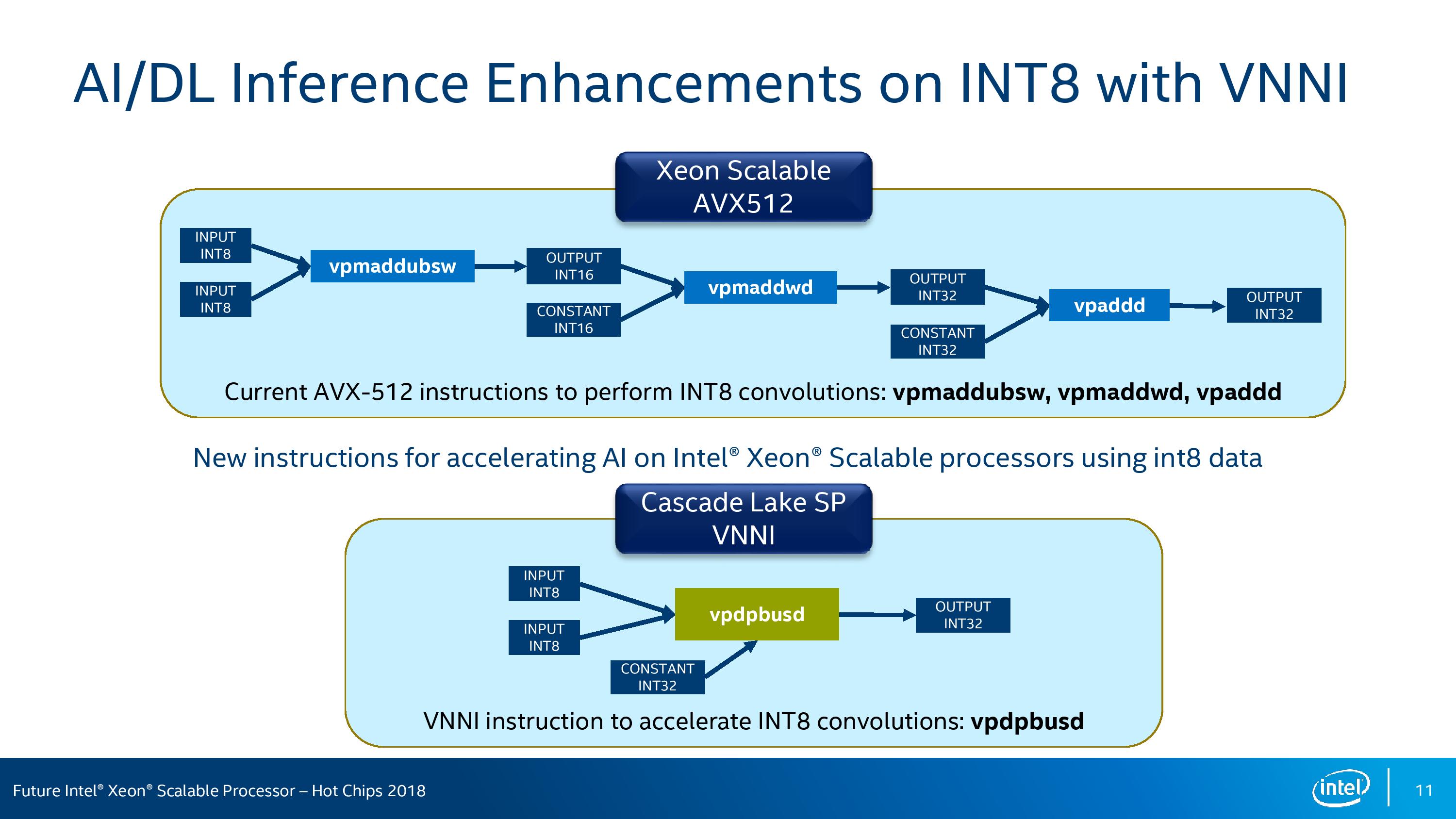
The key part from Intel here is that with the right data-set, these two instructions will improve the number of elements processed per cycle by 2x and 3x respectively.
Framework and Library for these new instructions will be part of Caffe, mxnet, TensorFlow, and Intel’s MKL-DNN.


31 Comments
View All Comments
HStewart - Monday, August 20, 2018 - link
It very possibility that Variant 1 is not volubility in the hardware designed but how OS developers use the code.GreenReaper - Monday, August 20, 2018 - link
Well, it's a problem for all software with secrets it wants to keep, and means of speculation involving access to them. The most common example of this is the OS/VMM.The core issue is that the speed of access to data is non-deterministic in the x86 model. Nothing in the original design said "you can't *try* to go faster than you would if you had to load everything only at the point that it came up" - indeed, doing so has been viewed as a feature for decades.
Meanwhile timing attacks have been viewed as relatively hard to exploit. But there are many ways in which a timing gadget may be constructed, this is arguably just a newly-discovered pattern commonly used by privileged software.
HStewart - Monday, August 20, 2018 - link
Unfortunately today we have increase of hackers that will try to take advantage of such features to hamper system. Which cause headaches for both CPU designers and OS designers.Also the following link as interesting statement about these attacks not being just Intel.
It actually states "This contradicts some early statements made about the Meltdown vulnerability as being Intel-only"
https://en.wikipedia.org/wiki/Meltdown_(security_v...
iwod - Monday, August 20, 2018 - link
When Zen 2 comes, which is going to be slightly later than CLake I think, please test Clake with all those security measures fix and see how it fare against AMD.moozooh - Monday, August 20, 2018 - link
So does this mean the Optane DIMMs won't be compatible with the consumer CPUs / chipset families? Cause I'd love to have it as a universal in-hardware RAM drive alternative with comparable latencies and IOPS performance but more convenience and far less compatibility issues.edzieba - Monday, August 20, 2018 - link
We've known that for quite some time: the Optane DIMMs require dedicated hardware in the processor (where the memory controllers are) which is only currently present in Xeon scalable CPUs.HStewart - Monday, August 20, 2018 - link
This is exactly wanted to here about the Spectrum - Meltdown stuff - we all know it that Intel has been under stress about this and the delay of 10nm - but some have reported that the hardware changes would be delay until 10nm - so this means that Intel does not have to have all 10nm to make those changes in hard. So 14nm++ or what every people is not same architecture as previous chips. To me it obvious that Intel has put fixing these security issues top priority.As for some of problems requiring OS/VMM - as a former OS developer, it very possible that volubility is in designed of OS - Intel has given OS developers like Microsoft, Apple - and unix base community software recommendations for changes in code to prevent them in current hard.
wpapolis - Monday, August 20, 2018 - link
“Showing the Ankle” and “drip feeding”? You r mixing your metaphors. You need to focus on one theme like ... “raising it’s skirt”, “showing more leg” ... u know ... like that! 👍 Another great article ... now let me get back to reading the rest! HahaKevin G - Monday, August 20, 2018 - link
Intel did do something tricky in that while LGA 3647 exposes 48 PCIe lanes, the HCC and XCC dies actually contain 64 lane PCIe controller. The 16 lanes are for on package accelerators or fabric. While I doubt Intel did increase this figures (or add an on-die UPI link), their wording appears to keep that possibility open.nirmal12 - Monday, October 8, 2018 - link
For those people expecting an IDF-like substantial talk about the chips. The question arising are how the SKUs will be separated, How product stack will look like etc. I also think Intel will be drip feeding information about Cascade Lake.