2nm
One of the core challenges that Rapidus will face when it kicks off volume production of chips on its 2nm-class process technology in 2027 is lining up customers. With Intel, Samsung, and TSMC all slated to offer their own 2nm-class nodes by that time, Rapidus will need some kind of advantage to attract customers away from its more established rivals. To that end, the company thinks they've found their edge: fully automated packaging that will allow for shorter chip lead times than manned packaging operations. In an interview with Nikkei, Rapidus' president, Atsuyoshi Koike, outlined the company's vision to use advanced packaging as a competitive edge for the new fab. The Hokkaido facility, which is currently under construction and is expecting to begin equipment installation...
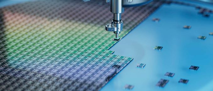
Applied Materials' New Deposition Tool Enables Copper Wires to Be Used for 2nm and Beyond
Although the pace of Moore's Law has undeniably slackened in the last decade, transistor density is still increasing with every new process technology. But there is a challenge with...
7 by Anton Shilov on 7/12/2024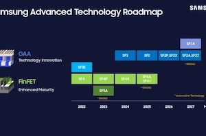
Samsung Foundry Unveils Updated Roadmap: BSPDN and 2nm Evolution Through 2027
Samsung this week has unveiled its latest process technologies roadmap at the company's Samsung Foundry Forum (SFF) U.S. The new plan covers the evolution of Samsung's 2nm-class production nodes...
10 by Anton Shilov on 6/13/2024TSMC: Performance and Yields of 2nm on Track, Mass Production To Start In 2025
In addition to revealing its roadmap and plans concerning its current leading-edge process technologies, TSMC also shared progress of its N2 node as part of its Symposiums 2024. The...
9 by Anton Shilov on 5/30/2024
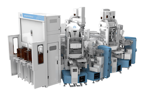
Rapidus Adds Chip Packaging Services to Plans for $32 Billion 2nm Fab
To say that the global foundry market is booming right now would be an understatement. Demand for leading-edge process technologies driven by AI and HPC applications is unprecedented, and...
12 by Anton Shilov on 5/24/2024
TSMC's Roadmap at a Glance: N3X, N2P, A16 Coming in 2025/2026
As announced last week by TSMC, later this year the company is set to start high-volume manufacturing on its N3P fabrication process, and this will be the company's most...
47 by Anton Shilov on 5/22/2024
Samsung Tapes Out Its First 3nm Smartphone SoC, Gets A Boost From Synopsys AI-Enabled Tools
This week Samsung Electronics and Synopsys announced that Samsung has taped out its first mobile system-on-chip on Samsung Foundry's 3nm gate-all-around (GAA) process technology. The announcement, coming from electronic...
8 by Anton Shilov on 5/3/2024
Samsung Foundry Update: 2nm Unveil in June, Second-Gen SF3 3nm Hits Production This Year
As part of Samsung's Q1 earnings announcement, the company has outlined some of its foundry unit's key plans for the rest of the year. The company has confirmed that...
4 by Anton Shilov on 5/1/2024
TSMC 2nm Update: N2 In 2025, N2P Loses Backside Power, and NanoFlex Brings Optimal Cells
Taiwan Semiconductor Manufacturing Co. provided several important updates about its upcoming process technologies at its North American Technology Symposium 2024. At a high level, TSMC's 2 nm plans remain...
0 by Anton Shilov on 4/25/2024
TSMC to Receive $6.6B Under US CHIPS Act, Set to Build 2nm Fab in Arizona
TSMC has entered into a preliminary agreement with the U.S. Department of Commerce, securing up to $6.6 billion in direct funding and access to up to $5 billion in...
23 by Anton Shilov on 4/8/2024
Rapidus to Get $3.9 Billion in Government Aid for 2nm, Multi-Chiplet Technologies
Rapidus, a Japan-based company developing 2nm process technology and aiming to commercialize it in 2027, will receive a huge government grant for its ongoing projects. The Japanese government will...
10 by Anton Shilov on 4/2/2024
Marvell's 2nm IP Platform Enables Custom Silicon for Datacenters
Marvell this week introduced its new IP technology platform specifically tailored for custom chips for accelerated infrastructure made on TSMC's 2nm-class process technologies (possibly including N2 and N2P). The...
0 by Anton Shilov on 3/8/2024
Tenstorrent Licenses RISC-V CPU IP to Build 2nm AI Accelerator for Edge
Tenstorrent this week announced that it had signed a deal to license out its RISC-V CPU and AI processor IP to Japan's Leading-edge Semiconductor Technology Center (LSTC), which will...
22 by Anton Shilov on 2/28/2024
Arm and Samsung to Co-Develop 2nm GAA-Optimized Cortex Cores
Arm and Samsung this week announced their joint design-technology co-optimization (DTCO) program for Arm's next-generation Cortex general-purpose CPU cores as well as Samsung's next-generation process technology featuring gate-all-around (GAA...
3 by Anton Shilov on 2/22/2024
TSMC 2nm Update: Two Fabs in Construction, One Awaiting Government Approval
When Taiwan Semiconductor Manufacturing Co. (TSMC) is prepping to roll out an all-new process technology, it usually builds a new fab to meet demand of its alpha customers and...
38 by Anton Shilov on 1/19/2024
TSMC: Ecosystem for 2nm Chip Development Is Nearing Completion
Speaking to partners last week as part of their annual Open Innovation Platform forum in Europe, a big portion of TSMC's roadshow was dedicated to the next generation of...
20 by Anton Shilov on 10/12/2023TSMC: Importance of Open Innovation Platform Is Growing, Collaboration Needed for Next-Gen Chips
This year TSMC is commemorating 15 years of its Open Innovation Platform, a multi-faceted program that brings together the foundry's suppliers, partners, and customers to help TSMC's customers better...
4 by Anton Shilov on 10/12/2023
Rapidus Wants to Supply 2nm Chips to Tech Giants, Challenge TSMC
It has been a couple of decades since a Japanese fab has offered a leading-edge chip manufacturing process. Even to this day, none of the Japanese chipmakers have made...
19 by Anton Shilov on 7/26/2023
Samsung Updates Foundry Roadmap: 2nm in 2025, 1.4nm in 2027
Samsung Foundry revealed its latest process technology roadmap today at its annual Samsung Foundry Forum (SFF) 2023. The company's SF2 (2 nm-class) production node is on track for 2025...
4 by Anton Shilov on 6/27/2023
Intel to Spend Tens of Billions on New Fabs in Germany and Israel
Intel is spending tens of billions of dollars on new fabs in Arizona and Oregon, but the company's ambitions certainly do not end in the U.S. This month the...
28 by Anton Shilov on 6/21/2023


