Analyzing Intel-Micron 3D XPoint: The Next Generation Non-Volatile Memory
by Kristian Vättö, Ian Cutress & Ryan Smith on July 31, 2015 11:00 AM ESTThe Technology: How Does 3D XPoint Work?
The way 3D XPoint works is fundamentally very different from NAND. Whereas NAND defines bit values by trapping a varying number of electrons in an insulated floating gate, 3D XPoint is a resistance based technology that works by a bulk property change to alter the resistance level of a cell and thus differentiate between a 0 and 1.
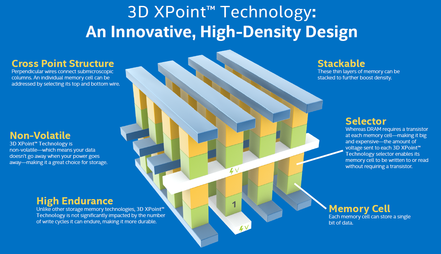
The 3D XPoint structure is very simple. It consists of a selector and memory cell, which sit in between a wordline and bitline (hence the "crosspoint" name). Applying a specific voltage on the wordline and bitline will activate a single selector and enables the cell underneath to be either written (i.e. a bulk property change in the memory cell material) or read (allows the current through to check whether the memory cell is in high or low resistance state). I suspect that write operations require a higher voltage than read because otherwise there might be a risk of triggering a bulk material change (i.e. write operation) while reading a cell. Intel and Micron wouldn't disclose any internal read/write voltages, but we were told that the voltages are considerably lower than in NAND, which requires ~20V for program/erase to create an electric field strong enough to tunnel electrons through an insulator. The lower voltages should, in turn, result in lower power consumption compared to DRAM and NAND.
As the name suggests, the cells can be stacked in a 3D fashion to further improve density and the first generation die that is currently sampling a a two-layer design. Two layers does sound few compared to 3D NAND that is already at 32 layers with 48 being close to production, but the way 3D XPoint array is built is fundamentally quite different.
3D NAND is manufactured by first depositing alternating layers of conducting and insulating materials on top of each other. It's only after all layers have been deposited that the "cell towers" are lithographically defined, followed by a high aspect ratio etch with the hole being filled by channel material to gain access to a memory cell in each layer. In 3D XPoint, however, each layer needs to be lithographically patterned and etched (i.e. repeating the same process for each layer) before another layer can be deposited, which does take away some of the economic benefits that 3D NAND has (i.e. very few lithography steps), but the 3D XPoint approach still provides higher density than what pure lithography based scaling would.
Intel and Micron said that scaling in future will happen through both lithography and 3D stacking of layers. Being scalable both horizontally and vertically is the key in enabling future-proof scalability because traditional Argon Fluoride based immersion lithography with multi-patterning is getting quite uneconomical at ~10nm and there is still no clear successor in the pipeline. The big bets seem to be on EUV and Intel-Micron confirmed that 3D XPoint will (unsurprisingly) be compatible with EUV lithography and the cell design can scale down to single digit nanometers without major impact on endurance/reliability (in fact, some aspects actually get better as the lithography is scaled down), but we are still at least a few years away from EUV being ready for use in high volume mass production. Initial EUV production will also focus on logic given the high equipment cost and because logic cannot be scaled vertically as easily as memory can due to heat issues.
In theory, 3D XPoint also supports multiple bits per cell, but that's not a path Intel and Micron are pursuing at the moment. While it's relatively easy to demonstrate multiple resistance levels in a lab, it's far more difficult to produce tens of thousands of wafers with each die having the necessary characteristics for proper multi-level cell operation. For comparison, it took nearly two decades before a second bit per cell was introduced to NAND, so for now Intel and Micron will focus on lithography and 3D scaling to increase density and cost efficiency, but multi-level cells may become a viable alternative in the future.
One of the big architectural differences to NAND is the fact that 3D XPoint is accessible at the bit-level. In NAND a whole page (16KB for the latest nodes) had to be programmed at once in order to save just one bit of data and to make matters worse you could only erase at the block level (a couple hundred pages at least). As a result, NAND requires sophisticated garbage collection algorithms for efficient performance, but regardless of the level of sophistication there is still performance degradation as a drive enters steady-state because of the inherent read-modify-write cycle that is needed to erase invalid pages within a block. With each cell being individually accessed 3D XPoint doesn’t necessarily require any garbage collection to work effectively, which simplifies the controller and firmware architecture, and even more importantly enables higher performance and lower power consumption.
I suspect that end products, especially storage focused, may still employ logical pages to reduce the tracking overhead because tracking data at a bit level would require a massive cache. However, Intel and Micron made it clear that today’s announcement was solely a technology announcement, so the companies declined to comment anything about upcoming products based on the new technology. That said, both are working on their own products with first commercial shipments scheduled for next year.
The Memory Cell: What's the Secret Behind 3D XPoint?
Section by Ian Cutress
At an array level, 3D XPoint operation is rather easy to understand, but what happens inside the memory cell during a bulk property change is a more complex issue. Personally, what comes to mind is that there are two ways in order to do this – physically adjust the properties of the cell with an external stimulus that adjusts the crystal structure, or chemically adjust the properties of the material used in the cell. During the discussions after the announcement, we were told categorically that this is not a phase change material, eliminating one potential avenue that it might be the change in the crystal structure of the cell producing the resistance change. This also makes a lot of sense, given the claims of a high durability where a constant crystal structure change could have affected the metal bonding between different parts of the cell as inter-structure atom lengths adjusting frequently. This leaves a chemical adjustment, or specifically the realignment in the electron structure of the bit in the cell, that promotes the resistance difference.
After some research, it’s worth talking about the types of technologies that could be being used here.
Spin-Crossover
From previous experience, my fingers automatically point to spintronics and the application of spin-crossover compounds. The short version of this means that a material can have two different resistance levels depending where exactly the electrons are in the electron levels of the structure, and an external stimulus (temperature, high voltage, magnetic field) can be used to switch between the two.
For the long answer, it is best to consider individual transition metal atoms. Depending on the local arrangement around the metal, the bonding orbitals of the metal are partially filled with electrons:
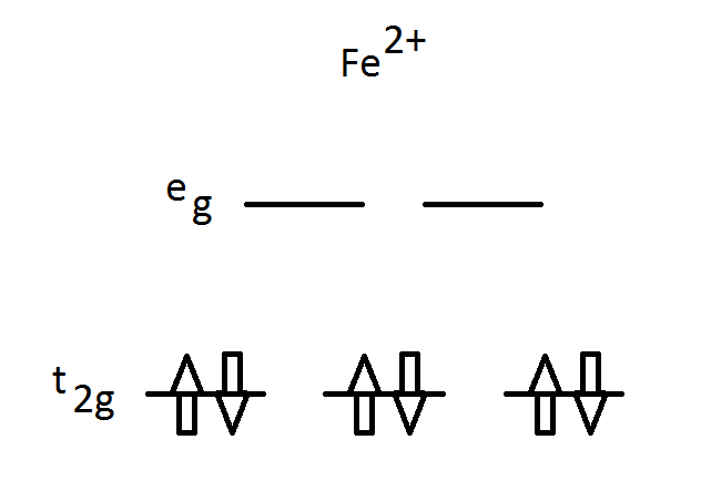
Here is an iron molecule in a 2+ environment, with its main bonding orbitals called t2g (lower energy) and eg (higher energy). Due to Pauli’s exclusion principle, each of the six electrons are paired into three orbitals and each pair of electrons has one ‘spin-up’ and one ‘spin-down’. This is the ground state, also known as the low-spin state as the total spin, S, is equal to zero, as each electron of spin 1/2 is cancelled out by the other electron having -1/2.
The other mode for this atom is the high-spin state where two electrons move to the higher bonding orbitals giving a total spin of S = 2:
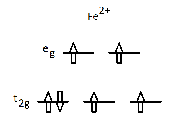
Due to an external stimulus, two of the electrons have flipped their spin and occupied the higher energy eg orbitals and this is officially a ‘metastable’ state. Depending the arrangement around the atom, this state could fundamentally be very stable and yet have wildly differing properties to the original ground state.
Extrapolating this out into a bulk material is fundamentally difficult. A quick look at research papers suggests that spin-crossover compounds can be directly applied between junctions and their resistance changed, but the chemical base for such operations in many papers are carbon nanotubes, graphene layers or organic chains.
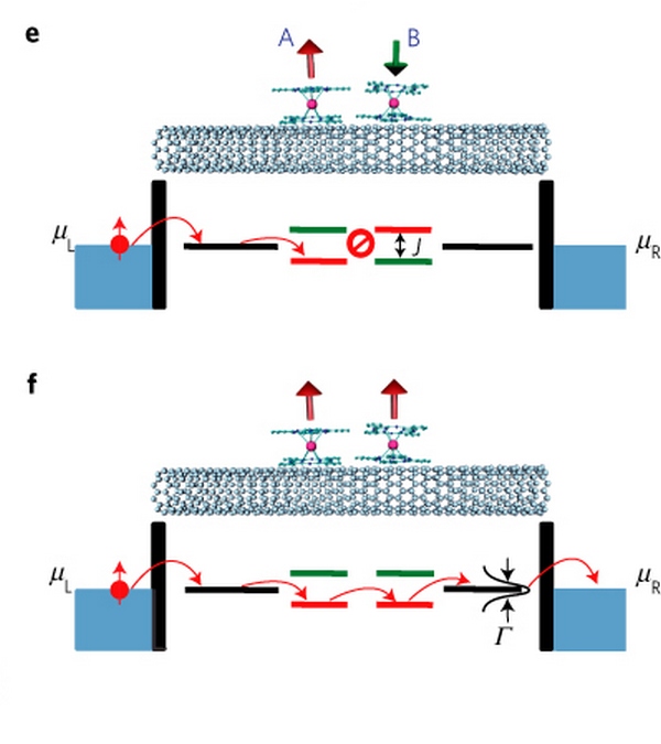
Image from M. Urdampilleta et al., Nature Materials, 10, 502 (2011)
In this paper, the orientation of the low-spin/high-spin states either affords conductivity between the two edges or does not, and depending on the metal in question will determine the exact nature, resistance, characteristics and/or stability of the platform. Intel will have had to have developed a material that is essentially programmed by voltage rather than any other stimulus, which adds to the complexity. Normally spin-crossover compounds have a specific temperature window as well which has a direct impact on stability as electrons may migrate from the high-state to low-state.
At this point, the scalability and fundamental material characteristics are the major barriers to large scale output of spin-crossover, particularly if nanotubes are required. If it was somehow extended to bulk metallic materials, as you bring an individual metal environment to bulk, band lines (and gaps) start to blur between simple orbital theories, so how it can be incorporated it into a cell is unknown. Intel is also stating that their technology is capable of multiple bits per cell, and the reality of spin-crossover arrangements can be blurred with electron tunnelling to achieve that effect.
Spin-Transfer Torque
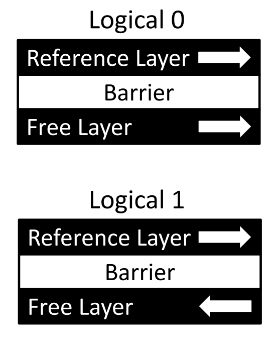
The STT method of memory cells relies on both the resistance between the states of the cell, as well as the ability to control magnetic fields within a cell itself. The short version is that if you adjust the magnetic alignment of a material, you can adjust the resistance and use it as a form of memory.
The long form for STT relies on a feature known as spin-polarised current. Electrons intrinsically have spin in two directions, up or down, and electric current typically consists of an even mix of these two, giving an overall un-polarised current (i.e. no overall spin direction majority). When an unpolarized current is passed through a thick layer of magnetic material, it causes the current to become polarised. If this polarised current then passes through a thin magnetic layer with a different density of electron states, the polarization of the current can cause the magnet to flip due to more electrons relaxing into states of opposite spin.
With the thick layer having a constant magnetic orientation and the thin layer (or the free layer) being able to flip, depending on the material, the resistance between the two combinations can act as a memory cell.
From Evaluating STT-RAM as an Energy-Efficient Main Memory Alternative, Kültürsay et. al.
Claimed benefits from STT methodologies revolve around energy consumption with it being lower to DRAM but with equivalent performance. Barriers to the technology depend on the ability to essentially create permanent magnets at such a small nanolithography note, and how placing many small magnets near each other (similar to bits on a HDD) might cause some of them to flip unexpectedly. Also with this method, it is unclear if it can scale beyond a simple binary bit per cell, and available research suggests that it requires a control transistor, which Intel has stated that 3D XPoint does not use.
Public history of STT development comes from a 1-megabit IC from Qualcomm on 45nm in 2011, and a 64-megabit module from Everspin in 2012 although no mention of a node.
Conductive Bridging
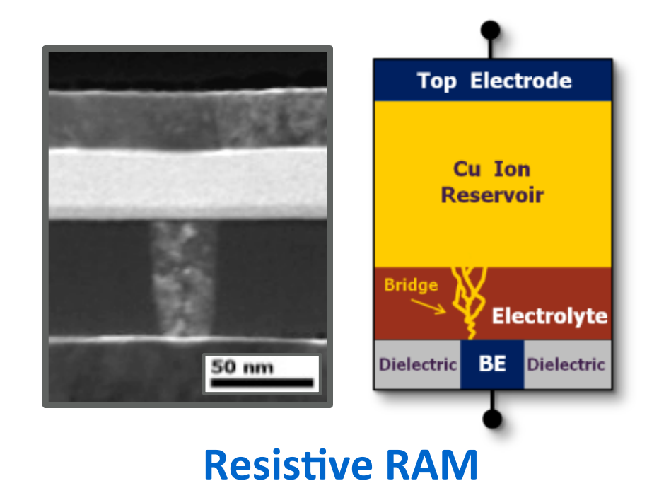
One of the easiest ways to adjust the resistance of a pathway is to block the path of electrons almost completely with a physical change. Conductive bridging technologies (or programmable metallization cells) rely on the creation of a nano-bridge between electrodes to reduce the resistance of a cell using a similar technique to electrolysis.
Within a CB cell, a thin film of electrolyte (historically a liquid, but can be a solid) is sat between an active and an inert electrode. When a negative bias is applied to the inert electrode the metal ions in the electrolyte are reduced to form metal atoms. When enough of these metal atoms are reduced and connected, it forms a wire between the two electrodes. In order to break the wire, the reverse potential difference is applied and the atoms in the wire are oxidized to become part of the electrolyte again. Ultimately the electrode-electrolyte-electrode combination is still conductive, but its resistance is higher than that of the situation where a wire is created.
Even discussing a brief overview of CB, for anyone familiar with electrolysis, brings up a large number of questions. First might be the use of liquids in a cell, but we should assume here that we might be dealing with mobile ions in a solid moving between intercalation points (spaces between a lattice/framework) anyway. But for me it comes to the growth of this ‘wire’. Typically growth via electrolysis is somewhat undirected – you are relying on the activity of various crystal planes to drive growth and ion diffusion is multi-directional, though there will be a slight bias towards the electrode depending on the crystal plane of growth. That leads to forked wires, similar to the way lightning works. When you do make a connection between the electrodes, or at least within electron tunneling distance, the resistance differential with the wire (from high resistance to low resistance) is large, but as the wire grows it will again decrease the resistance. This makes the wire method potentially multi-bit per cell, but as I mentioned before, growth control is hideously difficult. The other factor is that of reversing the process – typically the active electrode is made from the same material as the ions, meaning that the electrode itself could essentially dissolve. This creates a few headaches in research at least for durability.
To the benefit of CB, it theoretically scales to smaller than floating gate cells and the layout is simpler, with reported benefits in both power and performance by several orders of magnitude over current NAND.
Despite these issues and benefits, I might suggest that CB is currently the leading contender for the technology used in 3D XPoint. Subtle hints such as the official licensing of the technology by Micron in 2002, but also this slide in Micron’s Analyst conference in 2014 shows how they’ve overcome some of the issues I’ve listed above:

At the bottom here is the image above of a working cell along with a diagram showing how the bridging works. In order to facilitate the active electrode not being ‘eaten’ in reverse programming, we have a large ion reservoir to call on. The other electrode is also small in order to direct wire growth. As long as the electrolyte layer is small (several monolayers), read/write speeds can be quick and easy.
The Future
With all that being said, if we fast forward to Feb 2015, Micron released this slide at an analyst meeting:
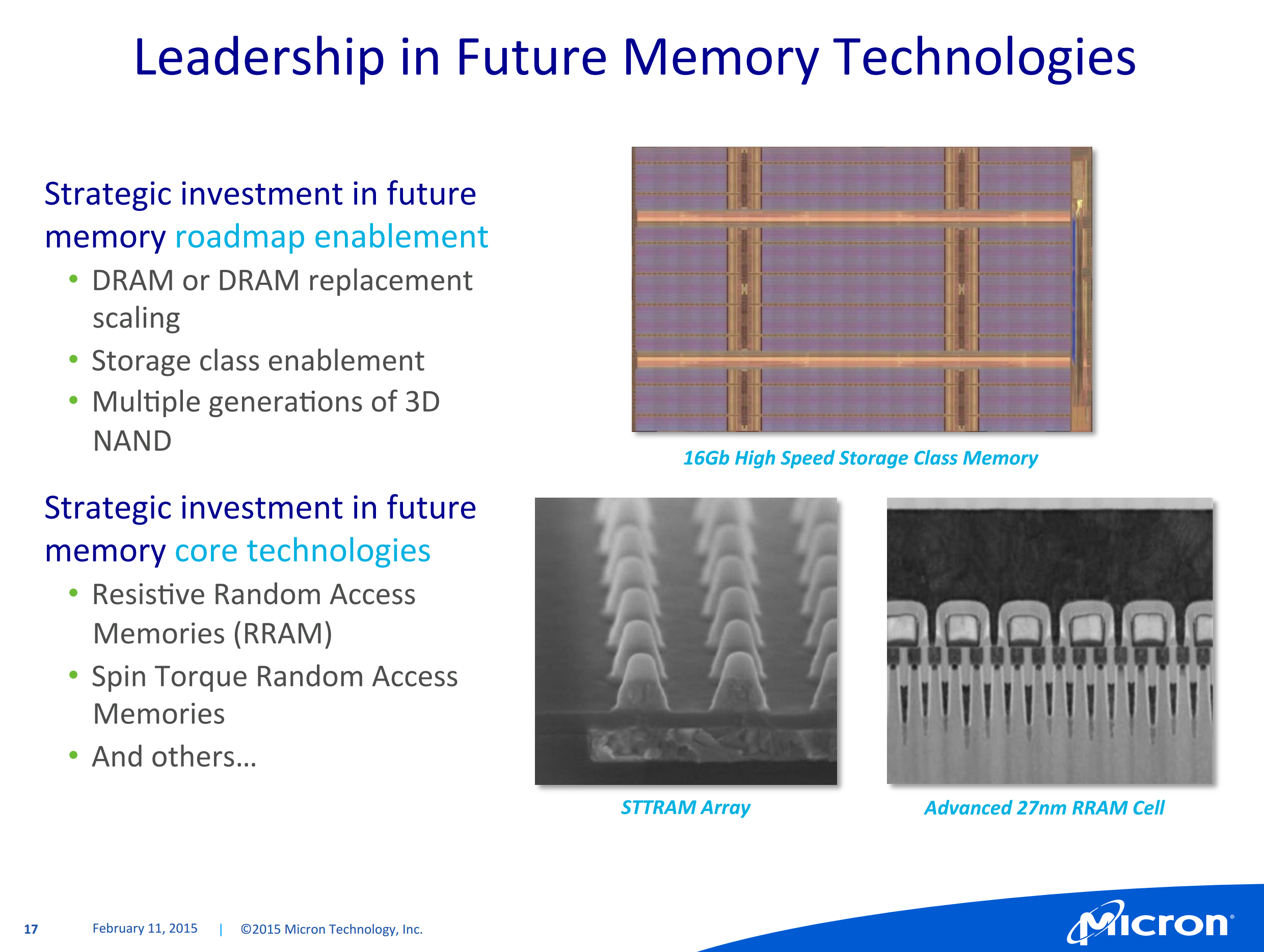
In the bottom half of this slide, it’s clear that Micron is looking into spin-transfer torque based memory on the left, and several analyst reports has suggested that the RRAM cell on the right is most likely that of CB technology. Within the 3D XPoint slides presented at the announcement this week, a number of analysts have also concluded that the selector per bit is most likely a diode in order to enable the appropriate characteristics for probing the resistance.
Given the fact that the announcement has stated that what is being done here is fundamentally different to previous attempts, and that the hardest part of producing 3D XPoint is the materials, I ultimately can’t judge on the exact specifics of what Intel and Micron are doing here, only that the conductive bridging method is most likely the method by which it is being done. Chances are the exact details will be kept close to Micron and Intel’s chest for a while as they are quoting a full decade research time from concept to product, which aligns from the 2002 licensing deal mentioned above for the conductive bridging method.


80 Comments
View All Comments
failquail - Friday, July 31, 2015 - link
Thinking about it, wouldn't an ideal use for this sort of memory be to use it as write-cache for storage devices? Almost as fast as RAM and does not need any sort of battery backup encase of power failures. Sounds perfect :)melgross - Friday, July 31, 2015 - link
I don't agree with the assumptions in the article about how this won't be a good replacement for current SSDs, because of cost. What I see here is that the prices,for,this arrive right at the price range of current SSDs. Yes, they are higher price SSDs, but still, not higher.It seems that the lesson of technology is lost here. All Tech becomes cheaper. It's almost as though the writers have forgotten that the first SSDs cost $3,600 for 32GB drives. HD prices have continued to fall, but not nearly as fast as that of SSDs.
Apple has almost all of their computers using SSDs, and that has certainly helped. They also use a major portion of the world's supply of NAND in their iOS devices. I'm not plugging Apple here, just pointing out that a major consumer company can affect usage and pricing dramatically.
If Apple, or some other major manufacturer decides that this Tech is just what they need, and begin to use it, then prices will begin to,drop,faster than otherwise thought.
I believe that this is a very good candidate for NAND drive substitution. And I feel as though it will begin happening more quickly than the writers here think it will.
Oxford Guy - Saturday, August 1, 2015 - link
Tech becomes cheaper as volume increases and manufacturing improves but SSD NAND will also become cheaper. So it remains to be seen how well this technology will drop in comparison with SSD NAND. Many people are still using 5400 RPM hard disks in their laptops so it is also not clear if there will be anything to compel regular people into buying something faster than an SSD and a higher price.abufrejoval - Friday, July 31, 2015 - link
I believe you’re falling into a marketing trap, when you imply that 32-layer Flash has 32x the capacity of planar flash (or 48-layer 48x capacity).When flash vendors talk about 3D Flash layers they are actually talking about process layers and it takes about 8 of them to implement a full logical storage plane. So 32 layer NAND simply has quad planar capacity and 48 layers six times the capacity of a planar chip at the same process size.
And since in the past 3D V-NAND was used to stay on the higher geometry node for endurance, actual capacity gain was even lower.
Intel/Microns bending technique was another way to retain surface area at lower geometries.
And as the V- in the V-NAND implies, you can’t stack silicon layers with complete freedom, even if processing cost were no issue. They were building terraces originally, something that the Toshiba 3D process avoids.
Still 100 or 1000 layers won’t happen on silicon, because that’s like building a skyscraper using mud bricks.
However, that’s not an issue with HP’s Memristor device, because that’s not a silicon process and layers of titanium dioxide can be slapped on top of each other without any crystalline alignment issues or deposition/etching limitations.
That is one of the enduring limitations of Xpoint vs. Memristor, the fact that it seems to remain a silicon based process, which means it doesn't allow anywhere the number of layers that a non-crystalline process can do.
And since the cost per layer is close to linear and high on silicon, that means it fails to deliver Moore's promise economically.
Kristian Vättö - Monday, August 3, 2015 - link
I'm well aware that 3D NAND uses a much larger lithography and the density per layer is far from planar NAND. I apologize if it reads differently, but that was unintentional, not a praise talk for 3D NAND.I think 100 layers will happen given that we are already close to 50 layers, but I agree that 1,000 layers would require a more significant change to the manufacturing process and materials.
abufrejoval - Friday, July 31, 2015 - link
My biggest fear with Xpoint is that Intel is attempting to create a de-facto monopoly around the NV-RAM space. They seem to have made a deal with HP for HP to delay the Memristor in return for some very favorable conditions on Xpoint, CPUs and whatever else HP needs to produce servers.An open price war between Memristor based and Xpoint based DDR4 DIMMs with hundreds of gigabytes if not terabyte capacity would have left half the industry bleeding to death, Intel would have lost against HP technologically, because the Memristor scales better in 3D, retains data indefinitely and has no endurance issues at all (also better latency, potentially even beating DRAM), but might have taken perhaps a little longer to get there.
And with Intel as an enemy and HP's current financial stand, there is a good chance they would have bled out on day 1 of that war.
So they agreed that is was better for both parties to delay the Memristor and give Intel a full run with Xpoint to recoup their investments and let HP regain some health and headstart against Lenovo, Dell and SuperMicro, who have no Memristor on the back burner to negotiate back channel rebates with Intel.
The only problem is that even if Xpoint looks like DDR4 RAM on the memory bus, it will require wear management, special initialization etc. via a control channel like SPI and in the BIOS.
Good luck trying to license that from Intel if you're a maker of ARM, AMD, p-Series or even z/Arch CPUs.
Intel gave up DRAM, because it was cut-throat commodity decades ago, but these days winds up making far less money off a standard big data server than DRAM manufacturers, even after they've pushed everybody else off the motherboard (Intel may make more profit, though).
XPoint not only gives them back the biggest slice on the server cake, and at a price they can move as close to DRAM as they want, while their production cost may actually be far lower, but it also eliminates all these pestly little ARM competitors as well as finishes big iron for once and for all for lack of a competitive memory solution.
What was probably a smart tactical move for HP, puts the future of the IT industry at risk because Intel has years of a practical, but thanks to Micron not legal, monopoly.
mdriftmeyer - Saturday, August 1, 2015 - link
Micron is on the verge of a hostile takeover of $23 Billion. This Joint Intel/Micron announcement came 3 days after that takeover bid.Sorry, but silicon is not the future, but the past. HP is in the driver seat with the Memristor. Once they fire Meg and hire an engineering board/ceo leveraging their IP will make Intel one unhappy camper.
lordken - Sunday, August 2, 2015 - link
Unfortunately I dont see HP (ES) is firing Meg anytime soon, she is going to HP ES as CEO...So I think that best chance to stuff her off was during separation where she should rather go to HP Ink rather then ES.Would not hold my breath for hope that HP would get good ceo, just look on couple of recent ceos we had...
Michael Bay - Sunday, August 2, 2015 - link
Memristor as technology is dead, HP is swithcing off from it. So there is no need for Intel to have any kind of dealing with them.Khenglish - Saturday, August 1, 2015 - link
I struggle to see the purpose of this memory. While flash is much slower, latency is limited by the controller. If you put this 3d XPoint memory in an SSD, you gain very little in performance since the controller was the bottleneck anyway. Flash manufacturers can get much higher performance from the memory out of a NOR design at the cost of some density, but they don't do it because again the controller is the issue. All I really see this being used for is business applications where flash memory's endurance is too low to be suitable.Also the term NAND only refers to the architecture of a memory system. I would not be surprised at all if 3D XPoint was also a NAND architecture. You might want to call the current tech flash or floating gate instead.