The Apple Watch Review
by Joshua Ho & Brandon Chester on July 20, 2015 8:00 AM EST- Posted in
- Wearables
- Apple
- Mobile
- Apple Watch
Apple S1 Analysis
One of the biggest issues with the smartwatch trend that I’ve seen is that as a result of most companies entering the market with smartphone backgrounds, we tend to see a lot of OEMs trying to shove smartphone parts into a smartwatch form factor. There have been a lot of different Android Wear watches, but for the most part everything seems to use Qualcomm’s Snapdragon 400 without the modem. Even though A7 is relatively low power for a smartphone, it’s probably closer to the edge of what is acceptable in terms of TDP for a smartwatch. Given that pretty much every Android Wear watch has around a 400 mAh battery at a 3.8 or 3.85 volt chemistry to attempt to reach 1-2 days of battery life and a relatively large PCB, the end result is that these smartwatches are really just too big for a significant segment of the market. In order to make a smartwatch that can scale down to sizes small enough to cover most of the market, it’s necessary to make an SoC specifically targeted at the smartwatch form factor.
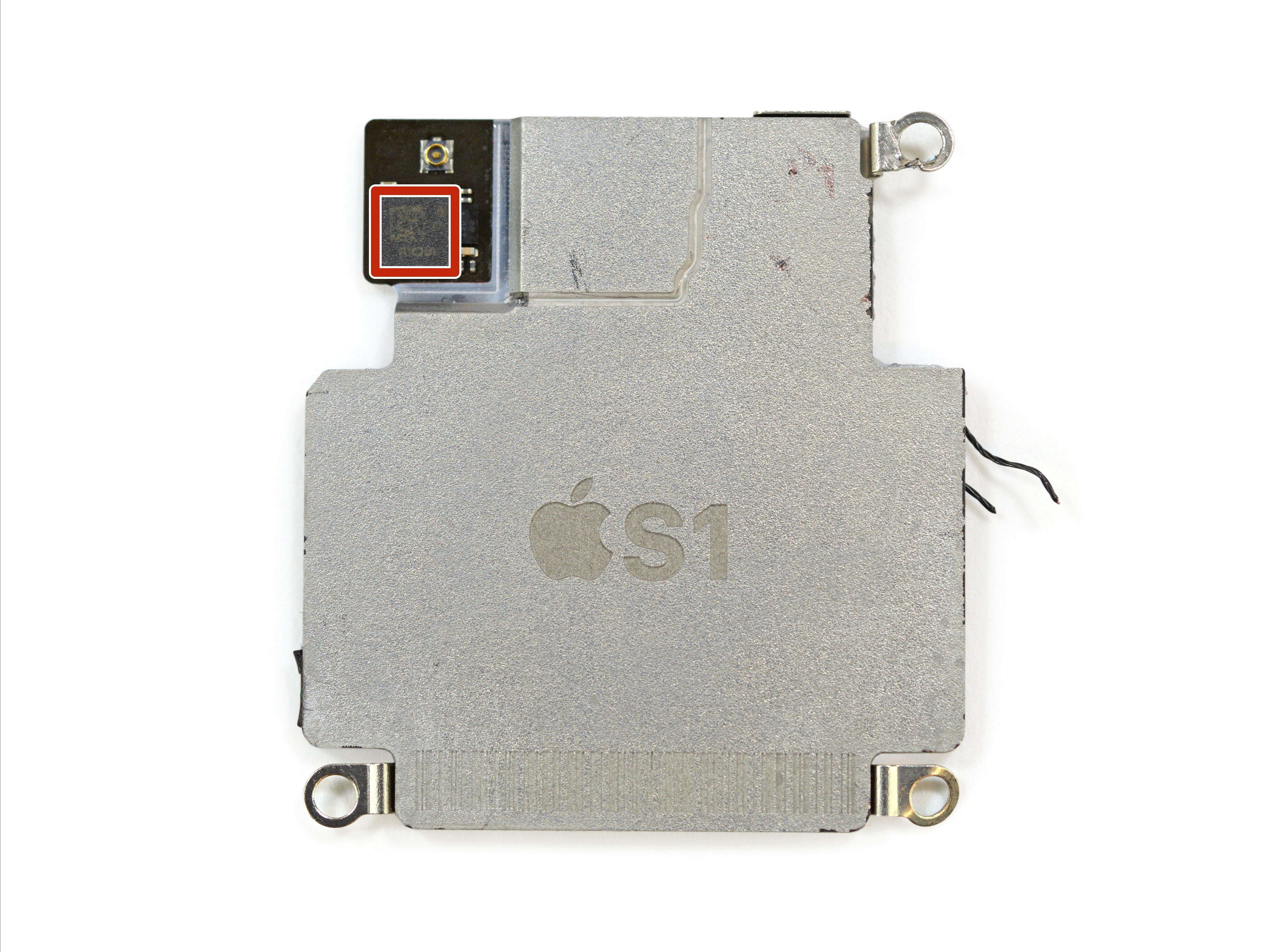
Capped Apple S1 SoC (Image Courtesy iFixit)
The real question here is what Apple has done. As alluded to in the introduction, it turns out the answer is quite a bit. However, this SoC is basically a complete mystery. There’s really not much in the way of proper benchmarking tools or anything that can be run on the Watch to dig deeper here. Based on teardowns, this SoC is fabricated on Samsung’s 28nm LP process, although it’s not clear which flavor of LP is used. It’s pretty easy to eliminate the high power processes, so it’s really just a toss-up between HKMG and poly SiON gate structure. For those that are unfamiliar with what these terms mean, the main difference that results from this choice is a difference in power efficiency, as an HKMG process has less leakage power. Given how little cost is involved in this difference in process compared to a move to 20/14nm processes, it’s probably a safe bet that Apple is using an HKMG process here especially when we look at how the move from 28LP to 28HPm at TSMC dramatically affected battery life in the case of SoCs like Snapdragon 600 and 800.
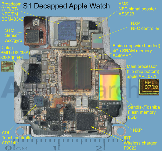
Decapped & Labeled S1 SoC (Image Courtesy ABI Research)
We also know that binaries compiled for the watch target ARMv7k. Unfortunately, this is effectively an undocumented ISA. We know that Watch OS is built on iOS/Darwin, so this means that a memory management unit (MMU) is necessary in order to make it possible to have memory protection and key abstractions like virtual memory. This rules out MCU ISAs like ARMv7m even if it's possible to add an MMU to such an architecture, so it’s likely that we’re looking at some derivative of ARMv7-A, possibly with some unnecessary instructions stripped out to try and improve power consumption.
The GPU isn’t nearly as much of a mystery here. Given that the PowerVR drivers present in the Apple Watch, it’s fairly conclusive that the S1 uses some kind of PowerVR Series 5 GPU. However which Series 5 GPU is up to debate. There are reasons to believe it may be a PowerVR SGX543MP1, however I suspect that it is in fact PowerVR's GX5300, a specialized wearables GPU from the same family as the SGX543 and would use a very similar driver. Most likely, dedicated competitive intelligence firms (e.g. Chipworks) know the answer, though it's admittedly also the kind of information we expect they would hold on to in order to sell it to clients as part of their day-to-day business activities.
In any case, given that native applications won’t arrive until WatchOS 2 is released I don’t think we’ll be able to really do much in the way of extensive digging on what’s going on here as I suspect that graphics benchmarks will be rare even with the launch of WatchOS 2.
Meanwhile, after a lot of work and even more research, we're finally able to start shining a light on the CPU architecture in this first iteration of Apple's latest device. One of the first things we can start to look at is the memory hierarchy, which is information crucial to applications that require optimization to ensure that code has enough spatial and/or temporal locality to ensure that code is performant.
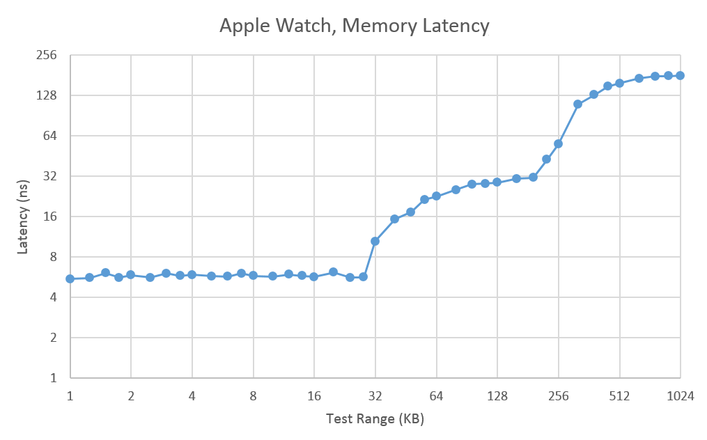
As one can see, there’s a pretty dramatic fall-off that happens between 28 and 64KB of “DRAM”, as we exit the local maximum of L1 data cache, so we can safely bet that the L1 data cache size is 32KB given current shipping products tend to fall somewhere between 32 and 64KB of L1 data cache. Given the dramatic fall-off that begins to happen around 224KB, we can also safely bet that we’re looking at a 256KB L2 combined cache which is fairly small compared to the 1-2MB shared cache that we might be used to from today’s large smartphone CPUs, but compared to something like an A5 or A7 it’s about right.
If Apple had just implemented the Cortex A7 as their CPU of choice, the obvious question at this point is whether they’ve really made anything “original” here. To try and dive deeper here, we can start looking past the memory hierarchy and looking closer at the machine itself. One of the first things that is obvious is that we’re looking at a CPU with a maximum frequency of 520 MHz, which is telling of the kind of maximum power that Apple is targeting here.
| Apple S1 CPU Latency and Throughput | ||||
| Instruction | Throughput (Cycles/Result) | Latency (Cycles/Result) | ||
| Loads (ldr reg,[reg]) | 1 | N/A | ||
| Stores (str reg,[reg]) | 1 | N/A | ||
| Move (mov reg, reg) | 1/2 | - | ||
| Integer Add (add reg, reg, imm8) | 1/2 | - | ||
| Integer Add (add reg,reg,reg) | 1 | 1 | ||
| Integer Multiply (mul reg,reg,reg) | 1 | 3 | ||
| Bitwise Shift (lsl reg,reg) | 1 | 2 | ||
| Float Add (vadd.f32 reg,reg,reg) | 1 | 4 | ||
| Double Add (vadd.f64 reg,reg,reg) | 1 | 4 | ||
| Float Multiply (vmul.f32 reg,reg,reg) | 1 | 4 | ||
| Double Multiply (vmul.f64 reg,reg,reg) | 4 | 7 | ||
| Double Divide (vdiv.f64 reg,reg,reg) | 29 | 32 | ||
Obviously, talking about the cache hierarchy isn’t enough, so let’s get into the actual architecture. On the integer side of things, integer add latency is a single cycle, but integer multiplication latency is three cycles. However, due to pipelining integer multiplication throughput can produce a result every clock cycle. Similarly, bitshifts take two cycles to complete, but the throughput can be once per clock. Attempting to interleave multiplies and adds results in only achieving half the throughput. We can guess that this is because the integer add block and the integer multiply block are the same block, but that doesn’t really make sense because of just how different addition and multiplication are at the logic level.
Integers are just half of the equation when it comes to data types. We may have Booleans, characters, strings, and varying bit sizes of integers, but when we need to represent decimal values we have to use floating point to enable a whole host of applications. In the case of low power CPUs like this one, floating point will also often be far slower than integers because the rules involved in doing floating point math is complex. At any rate, a float (32-bit) can be added with a throughput of one result per cycle, and a latency of four cycles. The same is true of adding a double or multiplying a float. However, multiplying or dividing doubles is definitely not a good idea here because peak throughput of multiplying doubles is one result per four clock cycles, with a latency of 7 clock cycles. Dividing doubles has a peak throughput of a result every 29 clock cycles, with a latency of 32 clock cycles.
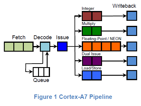
If you happen to have a webpage open with the latency and throughput timings for Cortex A7, you’d probably guess that this is a Cortex A7, and you’d probably be right as well. Attempting to do a load and a store together has a timing that indicates these are XOR operations which cannot be executed in a parallel manner. The same is true of multiplication and addition even though the two operations shouldn’t have any shared logic. Conveniently, the Cortex A7 has a two-wide pipeline that has similar limitations. Cortex A5 is purely single-issue, so despite some similarity it can't explain why addition with an immediate/constant value and a register can happen twice per clock.
Given the overwhelming amount of evidence at the timing level of all these instructions, it’s almost guaranteed that we’re looking at a single core Cortex A7 or a derivative of it at 520 MHz. Even if this is just a Cortex A7, targeting a far lower maximum clock speed means that logic design can prioritize power efficiency over performance. Standard cells can favor techniques and styles that would otherwise unacceptably compromise performance in a 2+ GHz chip could be easily used in a 520 MHz chip such as device stacking, sleepy stack layout, higher Vt selection with negative active body biasing, and other techniques that would allow for either lower voltage at the same frequency, or reduced capacitance in dynamic power and reduced static leakage. Given that Cortex A7 has generally been a winning design for perf/W metrics, I suspect that key points of differentiation will come from implementation rather than architecture for the near future. Although I was hoping to see Apple Watch on a more leading-edge process like 14LPP/16FF+, I suspect this will be deferred until Apple Watch 2 or 3.


270 Comments
View All Comments
everythingis1 - Tuesday, July 21, 2015 - link
Is anyone going to talk about that fact that these devices need 2 hands to operate. Doesn't that make the entire platform functionally irrelevant as anything other than a simple sensor? Am I completely crazy or is any smartphone, that can be operated with one hand for basic functionality, superior in every single way?deasys - Tuesday, July 21, 2015 - link
Actually, the Apple Watch can be operated 'no hands.' That's what Siri is all about.everythingis1 - Friday, July 24, 2015 - link
How do you activate Siri?Barilla - Tuesday, July 21, 2015 - link
Too bad one of the biggest features separating it from other smartwatches - the digital crown - becomes literally unusable if you decide to wear it on right hand. Yeah, some people do that...name99 - Tuesday, July 21, 2015 - link
LITERALLY unusable?http://www.imore.com/how-set-apple-watch-left-hand...
You mean the scheme Apple devised for this purpose doesn't work? Forgive me if I trust the opinions of various reviewers who have actually tried it over the opinion of someone who's never even touched an Apple watch...
nja4 - Tuesday, July 21, 2015 - link
I'm sort of on the anti-Apple hype train too, where reviewers are seem really expected to give Apple products overly positive reviews. However, I don't expect most people to share my opinions. The polish and appeal is so intense that I would bet most people would prefer their products over others. This review, as Ryan said, is going to be read by more than the core community, and I'm SO happy that Ryan responded in such a positive and discussion-oriented way. You're a great part of this community even when people are jerks about this sort of "obvious Apple bias."uhuznaa - Tuesday, July 21, 2015 - link
Nothing that draws 200 comments on Anandtech can be really pointless... As soon as reviews of Apple products will fizzle out here with five comments or so Apple will have lost it. But not sooner.Really, all you guys seem to be really obsessed with Apple. Even if you hate it, but you do care very much. Most reviews of smart watches draw much fewer comments...
Junereth - Tuesday, July 21, 2015 - link
this site really needs to make comments collapsible. it's incredible hard to navigate in here.SBD.3 - Tuesday, July 21, 2015 - link
I'd love to see the iWatch interface optimized on an iPhone. But as far as wearing a watch again, that ship has sailed.Tams80 - Tuesday, July 21, 2015 - link
A day for a smartwatch is just about bearable, just as it is a smartphone. More battery runtime is always better, but two to three days at moderate usage is the point at which I would be happy (basically, the ability to last a weekend away, where power is not easy to come by). One thing to take into account though, is that the smartphone takes priority. If there is only one charging point, the smartwatch gets left out, and therefore becomes useless.As for the review, I have some issues:
You haven't tried many watches, and by the sounds of it, none to the same extent as the Apple Watch. If that is the case, then I don't think you are qualified to make a comparison to them, as a professional reviewer. Further, you didn't even mention the Alcatel OneTouch Watch; the most apt comparison, as it also works with iPhones. As you clearly spent so much time of this review, you could have at least picked one up. They are cheap, but you also work for the well respected technology site; they might have even sent you one for free!
"The Apple Watch on the other hand doesn’t suffer from discomfort issues at all, and in this regard, Apple has arguably pushed the industry forward."
You do know that there are smartwatches out there that take standard watch straps? You do know that there are countless different designs of standard watch straps?
Finally, two specific points that really grated my gears (especially coming from someone who I expect to technologically knowledgeable):
"The ergonomic annoyances involved with wearing a wristwatch strongly outweighed whatever functionality it provided."
What ergonomic annoyances? The watch goes on your wrist, and in many cases never needs to come off. In return watches tell the time, often the date and day, and sometimes more. How is glancing at a watch less ergonomic than getting your phone out of wherever it is and checking it?
"wireless charging behaves differently from wired charging" - Total fluff, and no shit Sherlock.
So, to summarise. I think that while this was a good technical review of the Apple Watch, as a product review in general, it was very poor. The author let their personal view cloud his judgement too much, and comparisons were, well basically non-existent. If you didn't intend it to be a product review, then remove the product review sections. I expect much better from AnandTech.