Intel Xeon E5 Version 3: Up to 18 Haswell EP Cores
by Johan De Gelas on September 8, 2014 12:30 PM ESTThe Magic Inside the Uncore
We were already been spoiled by Ivy Bridge EP as it implemented a pretty complex uncore architecture. With Haswell EP, the communication between memory controllers, LLC, and cores has become even more intricate.
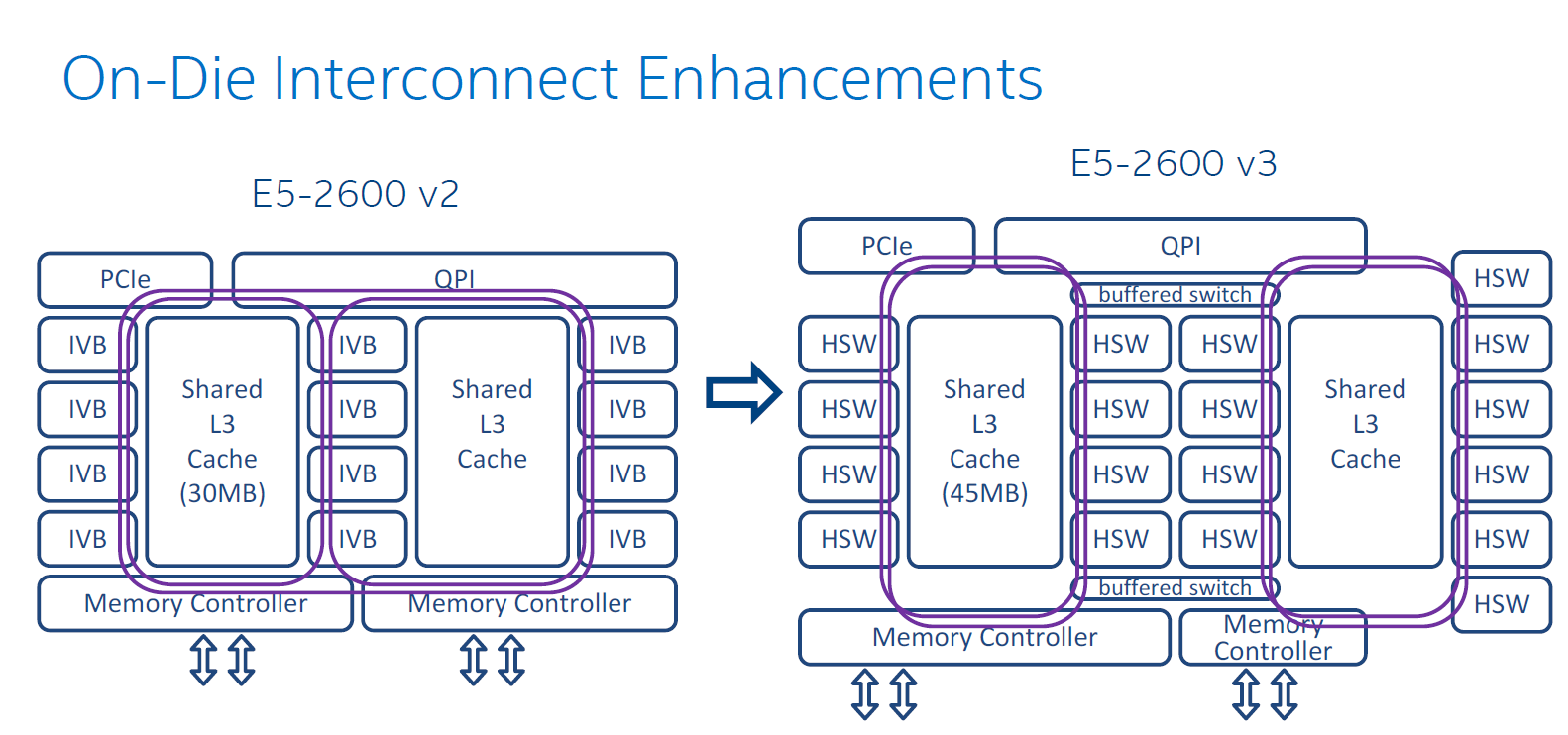
The Sandy Bridge EP CPU consisted of two columns of cores and LLC slices, connected by a single ring bus. The top models of the Ivy Bridge EP had three columns connected by a dual ring bus, with outer and inner rings as pictured above. The rings move data in opposite directions (clockwise/counter-clockwise) in order to reduce latency by allowing data to take the shortest path to the destination. As data is brought onto the ring infrastructure, it must be scheduled so that it does not collide with previous data.
The 14 and 18 core SKUs now have four columns of cores and LLC slices, and as a result scheduling gets very complicated. Intel has now segregated the dual ring buses and integrated two buffered switches to simplify scheduling. It's somewhat comparable with the way an Ethernet switch divides a network into segments. Each ring can act independently, and as result the effective bandwidth increases, which is especially helpful when FMA/AVX instructions are working on 256-bit chunks of data.
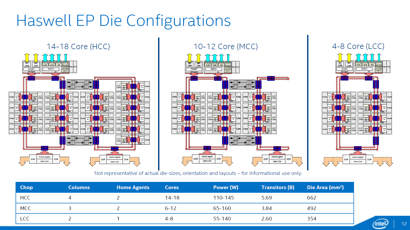
In total there are now three different die configurations. The first one, from four up to eight cores, is very similar to the lower count Ivy Bridge EPs. It has one dual ring, two columns of cores, and only one memory controller. The LLC cache is smaller on this die and has a lower latency.
The second configuration supports 10-12 cores and is a smaller version of the third die configuration that we described above. These dies have two memory controllers. The blue points indicate where data can jump onto the ring buses. Note that the die configurations are not symmetrical. For example an 18-core CPU has 8 cores (4-4) and 20MB LLC on one side, with 25MB LLC and 10 cores on the other. The middle configuration drops six to eight of the cores on the right ring, with an associated amount of LLC.
Data/instructions of one core are not stored in the adjacent cache slice. This could have lowered latency in some cases but it can create hotspots. Data is stored based on the physical address, ensuring all LCC cache slices are uniformly accessed. Transactions take the shortest path.
Rings are one of the entities that work on a separate voltage and frequency, just like cores. So if more I/O or coherency messaging is going on than processing, power can be dynamically allocated to speed up the rings.
Cache Coherency
The Home Agents are used for cache coherency and requests to DRAM. In dies that have two memory controllers, each home agent will use two channels. In dies that have one memory controller, each home agent will address four channels. While the smaller dies have faster LLC caches, Intel estimates that the second memory controller will extract 5% to 10% more bandwidth.
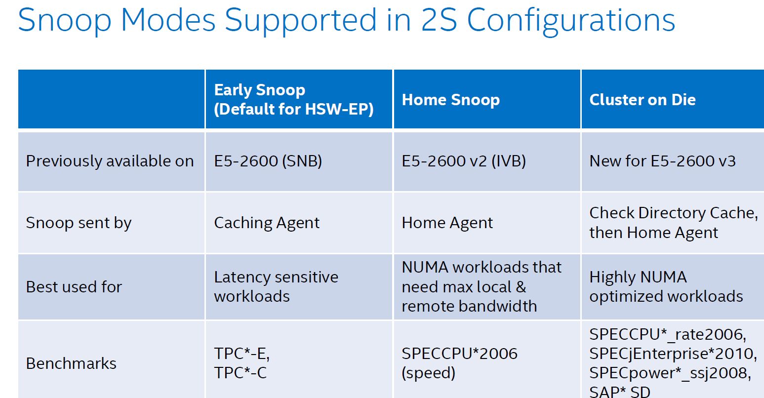
The two socket Haswell EP supports three snooping modes as you can see below. The first, Early Snoop, was available starting with Sandy Bridge EP models. With Ivy Bridge EP a second mode, Home Snoop, was introduced. Haswell EP now adds a third mode, Cluster on Die.
These snoop modes can be set in the BIOS.
Ivy Bridge used home snooping and had a directory in memory. The latest Xeon has directory caches (about 14KB) in each Home Agent. This directory cache keeps track of the contested cache lines to lower cache-to-cache transfer latencies. Another result is that directory updates in memory are less frequent and there are less broadcast snoops. Cluster On Die mode is the latest addition to the coherency protocols.
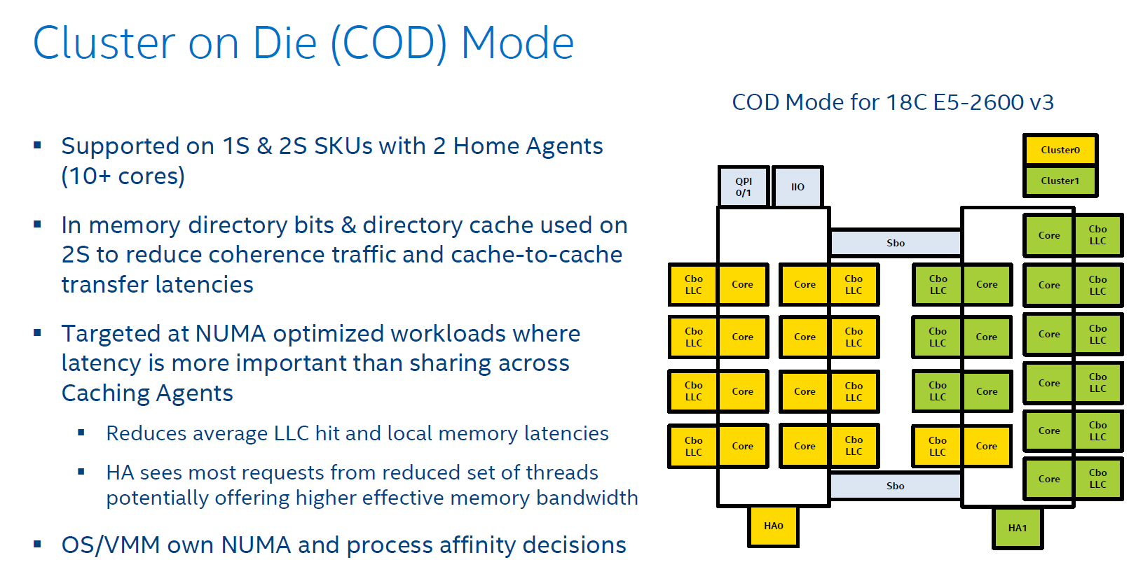
Cluster On Die can be understood as if you split the CPU and LLC into two parts that behave like two CPUs in NUMA. The OS is presented two affinity domains. As a result, the latency of LLC is lowered, but the hitrate is slightly lower. However if your application is NUMA aware, data and instructions are kept close to the part of the CPU that is processing them.
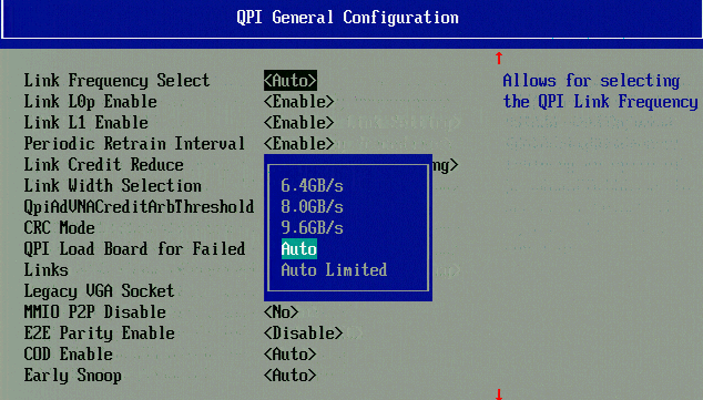
Higher QPI speeds, also notice the "COD" and "Early snoop" option.
And finally, QPI has been sped up to 9.6 GT/s, from 8 GT/s (as you can see in the BIOS shot).
More improvements
The list of (small) improvements is long and we have not been able to test all of them out. But here is an overview of what also improved
- Lower VM Entry/exit latency. The latency of going and forth to the Hypervisor has been improved compared to Westmere. Sandy Bridge slightly increase this compared to Westmere.
- VMCS shadowing. De VM Control Structure can be exposed to hypervisors running on top of the main hypervisor. So you get VT-x inside your nested hypervisor
- EPT Access and Dirty Bits. This makes it easier to move memory pages around, which is essiential for Live Migration / vMotion
- Cache monitoring (CMT) & allocation technology (CAT). CMT allow you to "measure" if a certain Virtual machine hogs the LLC . In certain SKUs is possible have control over the placement of data in the last-level cache.
Most of the improvements listed are specific for virtualized servers. However, cache allocation monitoring is also available for "native" OS.


85 Comments
View All Comments
LostAlone - Saturday, September 20, 2014 - link
Given the difference in size between the two companies it's not really all that surprising though. Intel are ten times AMD's size, and I have to imagine that Intel's chip R&D department budget alone is bigger than the whole of AMD. And that is sad really, because I'm sure most of us were learning our computer science when AMD were setting the world on fire, so it's tough to see our young loves go off the rails. But Intel have the money to spend, and can pursue so many more potential avenues for improvement than AMD and that's what makes the difference.Kevin G - Monday, September 8, 2014 - link
I'm actually surprised they released the 18 core chip for the EP line. In the Ivy Bridge generation, it was the 15 core EX die that was harvested for the 12 core models. I was expecting the same thing here with the 14 core models, though more to do with power binning than raw yields.I guess with the recent TSX errata, Intel is just dumping all of the existing EX dies into the EP socket. That is a good means of clearing inventory of a notably buggy chip. When Haswell-EX formally launches, it'll be of a stepping with the TSX bug resolved.
SanX - Monday, September 8, 2014 - link
You have teased us with the claim that added FMA instructions have double floating point performance. Wow! Is this still possible to do that with FP which are already close to the limit approaching just one clock cycle? This was good review of integer related performance but please combine with Ian to continue with the FP one.JohanAnandtech - Monday, September 8, 2014 - link
Ian is working on his workstation oriented review of the latest XeonKevin G - Monday, September 8, 2014 - link
FMA is common place in many RISC architectures. The reason why we're just seeing it now on x86 is that until recently, the ISA only permitted two registers per operand.Improvements in this area maybe coming down the line even for legacy code. Intel's micro-op fusion has the potential to take an ordinary multiply and add and fuse them into one FMA operation internally. This type of optimization is something I'd like to see in a future architecture (Sky Lake?).
valarauca - Monday, September 8, 2014 - link
The Intel compiler suite I believe already convertsx *= y;
x += z;
into an FMA operation when confronted with them.
Kevin G - Monday, September 8, 2014 - link
That's with source that is going to be compiled. (And don't get me wrong, that's what a compiler should do!)Micro-op fusion works on existing binaries years old so there is no recompile necessary. However, micro-op fusion may not work in all situations depending on the actual instruction stream. (Hypothetically the fusion of a multiply and an add in an instruction stream may have to be adjacent to work but an ancient compiler could have slipped in some other instructions in between them to hide execution latencies as an optimization so it'd never work in that binary.)
DIYEyal - Monday, September 8, 2014 - link
Very interesting read.And I think I found a typo: page 5 (power optimization). It is well known that THE (not needed) Haswell HAS (is/ has been) optimized for low idle power.
vLsL2VnDmWjoTByaVLxb - Monday, September 8, 2014 - link
Colors or labeling for your HPC Power Consumption graph don't seem right.JohanAnandtech - Monday, September 8, 2014 - link
Fixed, thanks for pointing it out.