An Introduction to Semiconductor Physics, Technology, and Industry
by Joshua Ho on October 9, 2014 3:00 PM EST- Posted in
- Semiconductors
- CMOS
- Physics
- Industry
- Technology
I must confess that until recently, I wasn’t well-versed in semiconductor physics or technology. While it’s rather easy to understand what a transistor does and some of the terminology thrown around, going deeper was tough. A great deal of the information on the internet is simply too cryptic to understand, even for those that want to learn. Seeing as how this site is all about the results of semiconductor physics and technology, this was the best place to share the knowledge that I've acquired.
Bandgap In Semiconductor / Pieter Kuiper
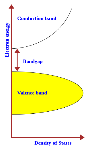
The simplest place to start is the materials. Silicon is incredibly important as a material in the industry because it’s a semiconductor. Of course, the name is self-explanatory, but there’s more to it. The key here is the band structure. Band structure refers to the “bands” of energy levels that form due to the sheer number of orbital states that can be occupied in molecules. Those that understand how electron orbitals work will point out that each energy level is discrete, but due to the sheer number of orbital configurations, a seemingly continuous distribution of energy can be seen. However, relatively large gaps still exist; known as a band gap, these are an energy state that an electron cannot occupy.

Band Filtering Diagram / Nanite
The question now is why this matters. The reason why it does matter is because of the Fermi level, or EF in the photo above. The Fermi level refers to the total chemical potential energy for a system of electrons at absolute zero. If the band lies above the Fermi level, electrons in the band can be delocalized from the atom, which means that it can carry current. This band is called a conduction band. If the band is below the Fermi level, this means that the electron is bound to an atom. This band would be a valence band.
Intrinsically, a semiconductor should have its Fermi level at the midpoint of the band gap. This is true of both insulators and intrinsic semiconductors, but a semiconductor’s band gap is extremely small. In fact, it’s small enough that electrons can jump the band gap as seen in the photo above because of thermal energy that will always exist in real world situations. While this property alone isn't particularly useful for digital logic, doping a semiconductor can have significant effects on the band structure. This means that the distribution of electrons in the valence band or conduction band will change.
This is where I have to introduce even more terminology. Depending on how the distribution is changed, a semiconductor is dubbed either a p-type or n-type semiconductor. If the band structure is such that free electrons are more easily generated, it becomes an n-type semiconductor. If the structure is such that electron “holes” are generated, it becomes a p-type semiconductor. In this case, electron holes refers to a place where an electron could exist, but doesn’t. Such a hole still conducts current. Look carefully at the p-type diagram once again. Because the valence band is so close to the Fermi level, electrons tend to stay in the valence band at lower orbitals. This is means that there are "holes" where an electron could be, which makes it a charge carrier. It's also worth noting that the diagram above isn't totally accurate, as doping normally introduces more bands instead of shifting their positions, but the concept is the same.
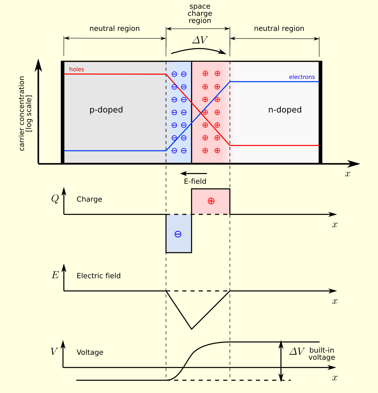
PN Junction Equilibrium / TheNoise / CC BY SA
What really makes things interesting is when a p-type and n-type semiconductor are placed next to each other. Because p-type semiconductors tend to have electron holes and n-type semiconductors tend to have an excess of electrons, there will be a diffusion of holes and electrons to try and equalize charge at the junction. Because of this diffusion process, the area around the junction becomes charged positively at the n-doped region and negatively at the p-doped region. This happens because the n-doped region is losing electrons, making the area positive while the p-doped region is losing holes, therefore becoming negative. The result is that an electric field is generated which opposes this diffusion and eventually reaches equilibrium. The area where this process occurs is called the depletion layer, as these ionized areas are stripped of charge carriers and therefore unable to carry current with the band structure that already exists.

PN Band / Saumitra R Mehrotra & Gerhard Klimeck / CC BY
This p-n junction is incredibly important in solid state electronics. In fact, the system we just described can be used as a diode, which is a device that only allows current to flow in a single direction. If a battery is connected with the positive terminal at the p-type semiconductor and the negative on the n-type semiconductor, the holes in the p-type and the electrons in n-type are all pushed towards the junction, which causes the depletion zone to shrink. This means that the electric field repelling the current decreases, and current is allowed to flow across the junction.


77 Comments
View All Comments
Kidster3001 - Wednesday, October 29, 2014 - link
Modern chips are connected with a C4 process (Controlled Collapse Chip Connect) The interconnect side is down, the bulk side is up. The heatsink is touching the back of the wafer.nand - Friday, October 10, 2014 - link
when i was 18 and in college i couldn't get head my over this stuff - after few years of growing up it makes perfect sense...sammycbvb - Friday, October 10, 2014 - link
Awesome article. I was waiting for a simplified explanation of Semiconductors and you've delivered.GT69 - Friday, October 10, 2014 - link
Great article for this old EE whose career was mostly in sales and marketing, but who has had a great love for PC's since the days of Apple II and CP/M. Nice that someone has taken the time and effort to give this generalized explanation even if some of the nit-pickers quibble over a typo or some specific detail. Until one has had to actually produce such a piece he/she should refrain from too much criticism. Easy and quick it ain't! Kudos...Dr.Neale - Saturday, October 11, 2014 - link
After many years of editing scientific / technical / medical journal articles, I tend to see the structural details as well as the informational content.To me, a typo is like a dead pixel. If it can be removed, it makes the image or storyline that much more immersive and enjoyable to behold.
The purpose is aiding the author in polishing the article to perfection, not fault-finding or nit-picking.
Like many tech enthusiasts, an editor brings a passionate pursuit of excellence to his craft and to his team.
Like many other commenters here, I see myself as making a small contribution, from time to time, to the AnandTech team.
Dr.Neale - Saturday, October 11, 2014 - link
P.S. I have also authored or coauthored numerous articles (and a textbook chapter) in the fields of medical physics and medical imaging, including invited review articles.So I offer my appeciation and congratulations to Josh Ho for gifting us with an article of such surpassing excellence.
dew111 - Friday, October 10, 2014 - link
This was a good review of my semiconductor physics course. But with less math :)Arnulf - Friday, October 10, 2014 - link
Very nice technical article, unlike the usual consumerist Apple et al chaff that has swamped this site as of lately!Senti - Friday, October 10, 2014 - link
Exactly my thoughts! It's really sad to see how level of this site has dropped significantly over years due to caring for more mindless crowd; certain reviewers doesn't bother to actually understand what they are reviewing and just pushing for faster time to post and more numbers (that are by large part are quite unrelevant).But articles like this show that hope is not lost here – great job, would love to see more articles like this.
SanX - Friday, October 10, 2014 - link
This is what puzzling for a long time: the wavelength of ArF laser is 192nm, the feature size of Core M processor is 14nm or 14 times smaller. With NA=1 you can focus into spot of the Airy size equal approximately to wavelength only. Using phase shift trick you can probably drop that size twice to 96nm. Using nonlinearity of photoresist you can drop twice more or to 49nm. My guess is that using titlting of laser (i do not get how it actually works) they can get 24nm. Adding water you can get 24 / 1.33=18nm. How they get 14nm and sometimes even 10nm what Samsung claims with just the optical lithography?