The Bay Trail Preview: Intel Atom Z3770 Tested
by Anand Lal Shimpi & Brian Klug on September 11, 2013 12:00 PM EST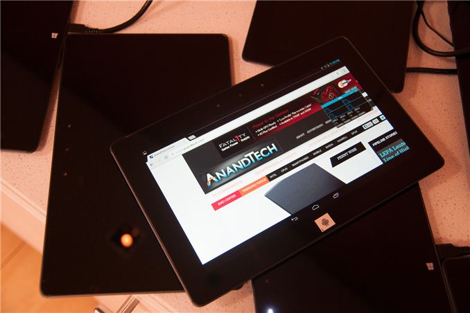
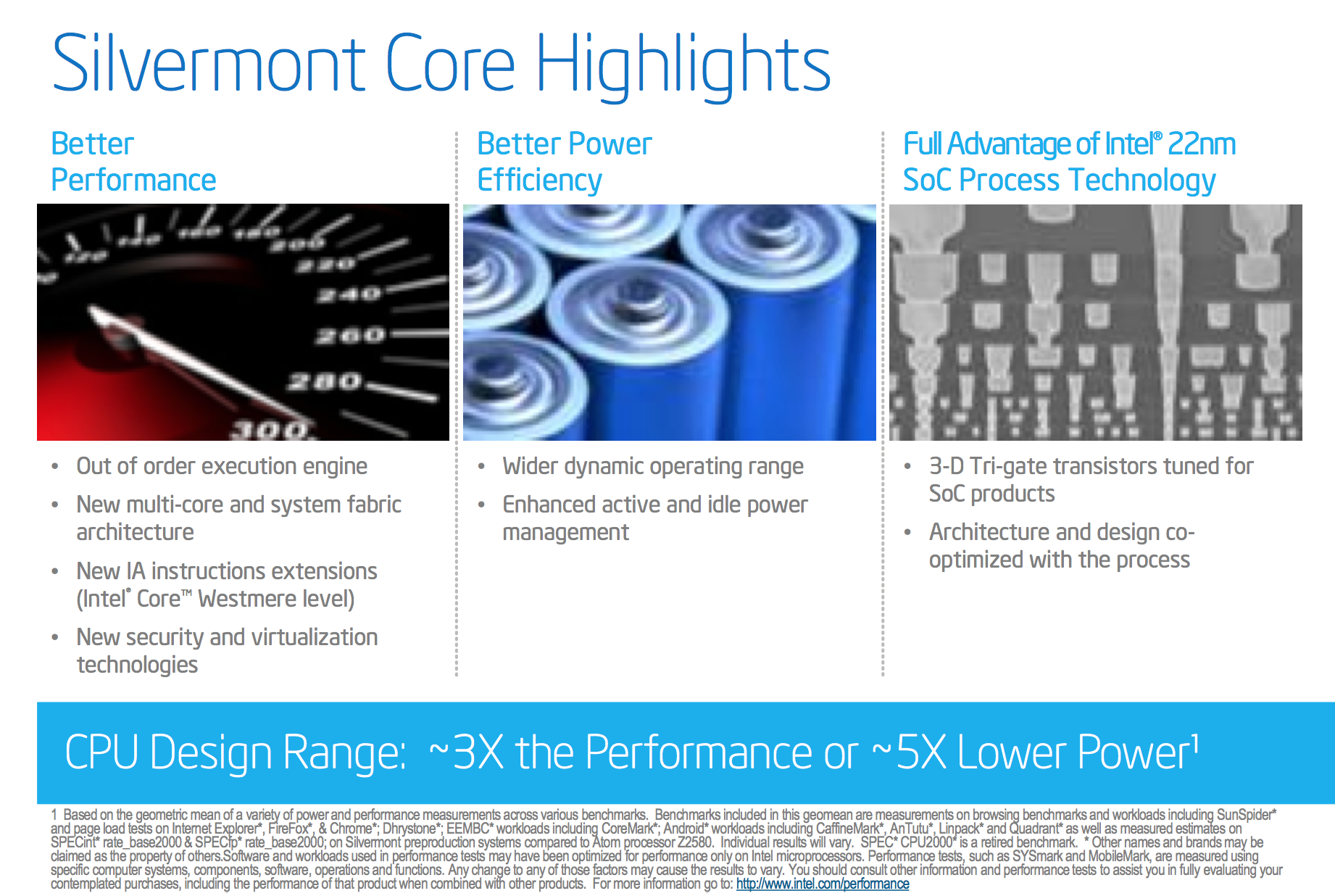
Earlier this year Intel unveiled Silvermont, its first true architectural update to Atom since its introduction in 2008. I won’t rehash Silvermont’s architecture here, but it’s designed to be a true test of Intel’s performance in the ultra mobile space. Leveraging Intel’s first 22nm SoC process and a very low power/efficient microarchitecture, Silvermont aims squarely at the latest Krait cores from Qualcomm and ARM’s Cortex A15.
Today Intel takes the next step forward, introducing the first tablet SoC based on Silvermont: Bay Trail.
Bay Trail takes up to four Silvermont cores, and for the first time in an ultra mobile Intel SoC pairs them with Intel’s own graphics IP. That’s right, rather than using a GPU block from Imagination Technologies, Bay Trail leverages the same GPU architecture as Ivy Bridge.
The first Bay Trail tablets will be shipping by the end of the year, across both Android and Windows 8.1. Intel expects Bay Trail to show up in tablets and 2-in-1s priced below $599, with everything above $599 falling under Haswell’s jurisdiction.
Bay Trail & Branding
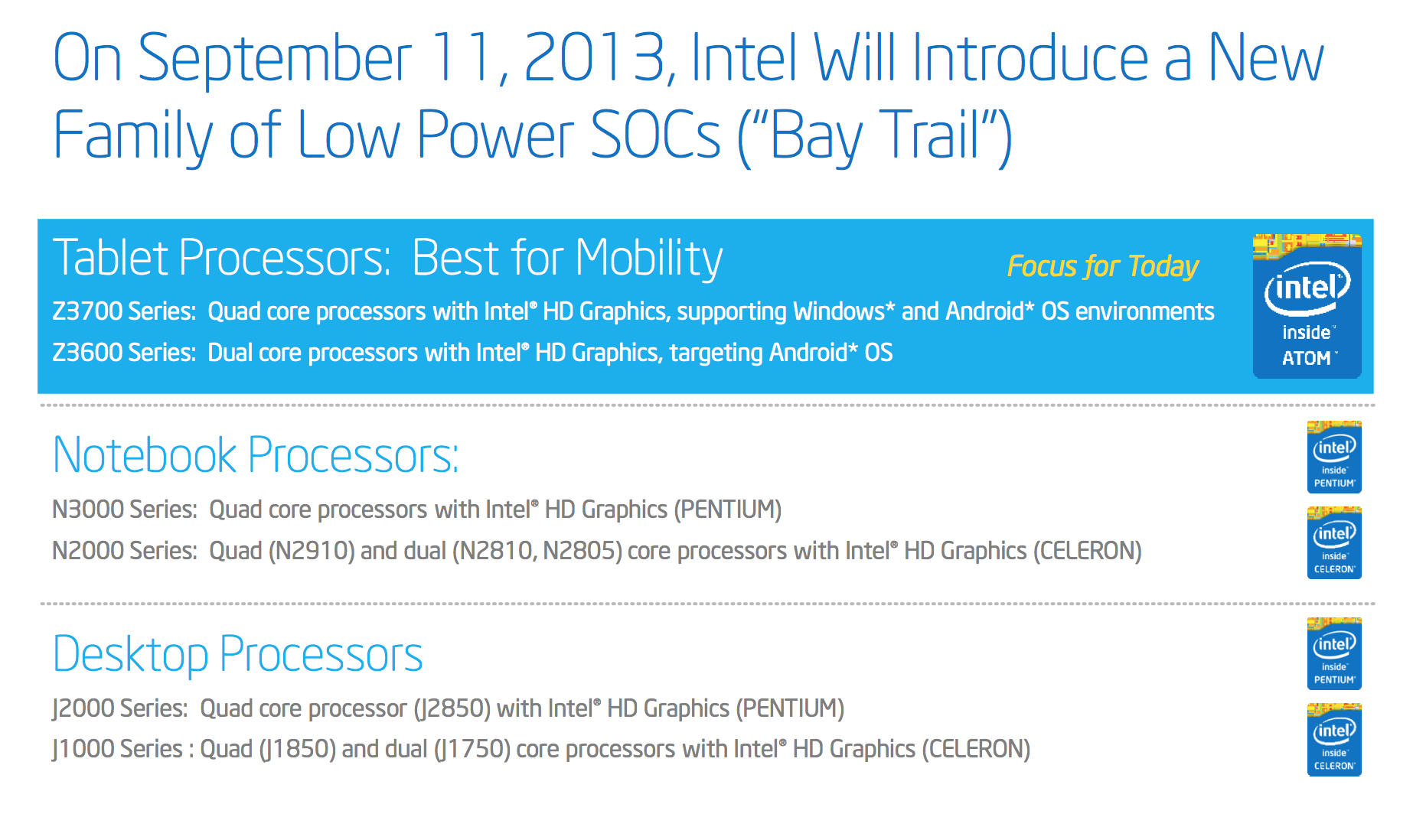
Bay Trail, like all Atom platforms before it, will be available in multiple form factors. Unlike the Atoms of yesterday however, the SoC will carry Pentium and Celeron branding when used in notebooks and desktops. Intel didn’t disclose too much about its Silvermont plans in other form factors other than some basic naming:
Basically notebooks ship under the Pentium N3000 & Celeron N2000 series, while desktops will carry Pentium J2000 & Celeron J1000 branding. All Pentium SKUs seem to be quad-core, while Celeron SKUs will be available in both dual and quad-core versions.
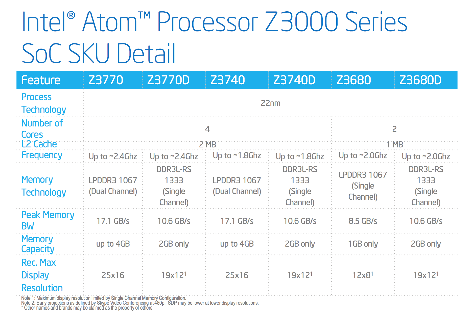
Thankfully Intel shied away from introducing the same complexity with its tablet focused Bay Trail parts. All Bay Trail tablet SKUs carry Atom branding. There’s the quad-core Z3700 series and the dual-core Z3600 series.
Although Intel offers both dual and quad-core Bay Trail SKUs, they are both based on the same single physical design. In other words, dual-core Bay Trail parts are just die harvested quad-core parts. Intel isn’t disclosing die size or transistor counts, which is ironic (and disappointing) given that Apple just disclosed both (or at least relative magnitude of one) for its A7 SoC.
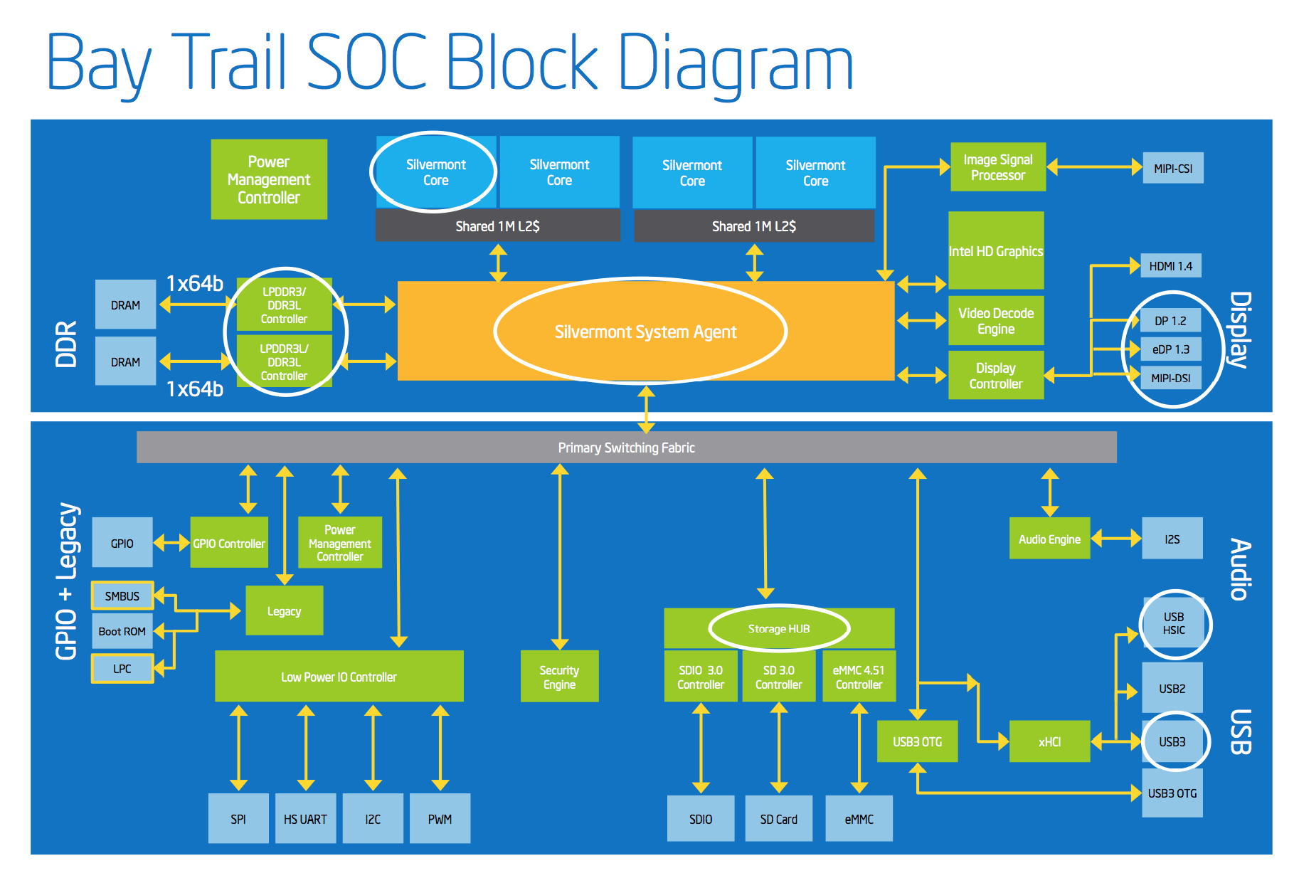
Internally, the Bay Trail design is pretty nice. There are either two or four cores enabled, each pair with a shared 1MB L2 cache (2MB total for a quad-core part). Intel is following the unfortunate lead of everyone else in the mobile industry and advertising max turbo frequencies exclusively.
Thankfully Intel hasn’t yet decided to obfuscate max non-turbo frequencies:
| Bay Trail Turbo Speeds | ||||||||
| Z3770 | Z3770D | Z3740 | Z3740D | Z3680 | Z3680D | |||
| Max turbo frequency | 2.39GHz | 2.41GHz | 1.86GHz | 1.83GHz | 2.0GHz | 2.0GHz | ||
| Max non-turbo Frequency | 1.46GHz | 1.5GHz | 1.33GHz | 1.33GHz | 1.33GHz | 1.33GHz | ||
In general you’re looking at 1.33GHz - 1.46GHz max non-turbo frequencies, with Bay Trail being able to turbo up to anywhere between 1.83GHz and 2.40GHz depending on SKU.
Although the core architecture is 64-bit in design, there will be no OS support for 64-bit Bay Trail at launch. Windows 8.1 with Connected Standby appears to still be 32-bit only, and obviously Android is 32-bit only at this point as well.
The memory interface is fairly ridiculous by mobile standards. You either get two 64-bit LPDDR3 channels (128-bit total width) or a single 64-bit DDR3L channel. In the case of the former, that’s the same memory bus width as Apple’s A5X/A6X line of SoCs as well as the standard Core i3/i5/i7 parts. Max supported memory frequency is 1066MHz in dual-channel LPDDR3 mode, or 1333MHz in single-channel DDR3L mode. The only benefit to the latter is really cost, as Bay Trail will purportedly show up in some very cheap devices.
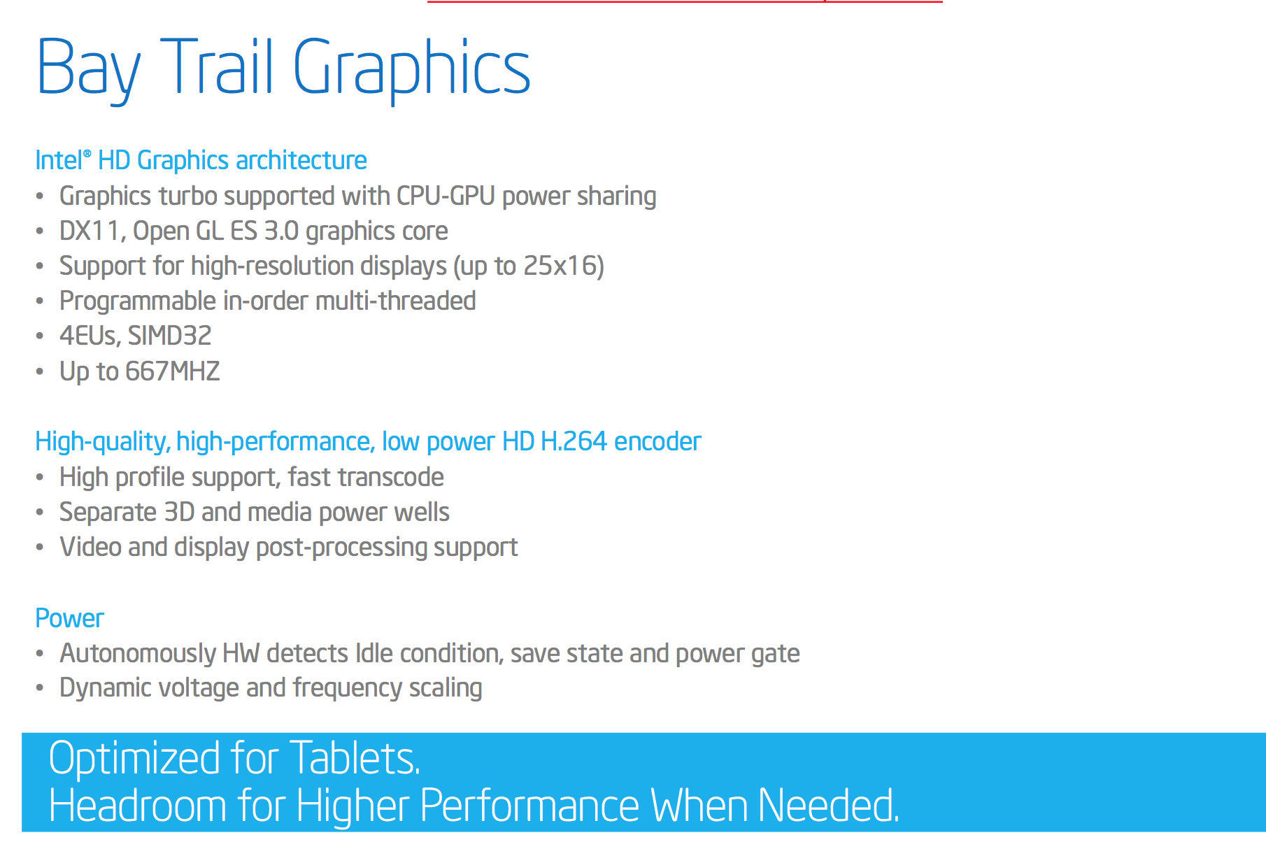
The GPU is Intel’s own Gen7 graphics core, a cut down implementation of what we first saw in Ivy Bridge. I suppose it’s premature to expect Merrifield, Bay Trail’s smartphone counterpart, to also use Intel’s own graphics core but it’s clear this is the direction Intel is headed in - and away from licensing IP from Imagination Technologies.
Rather than 16 EUs in the Ivy Bridge GT2 configuration (HD 4000), Bay Trail’s HD Graphics core ships with 4. The 4 EUs are otherwise effectively identical to what we found in Ivy Bridge. The GPU can dynamically scale frequency and share power between itself and the CPU cores. Minimum GPU frequency on Bay Trail is 311MHz and a max GPU frequency of 667MHz (or 688MHz for the DDR3L SKUs).
Intel is quick to point out that Bay Trail’s GPU supports DirectX 11 and OpenGL ES 3.0. Unfortunately this support list appears limited to Windows. Under Android, it’s unclear whether or not Bay Trail will ship with anything above OpenGL ES 2.0 support. The same goes for GPU accelerated Renderscript. Bay Trail supports up to 2560 x 1440 displays over eDP1.3/DP1.2, or 1080p over HDMI. Panel Self Refresh is also supported.
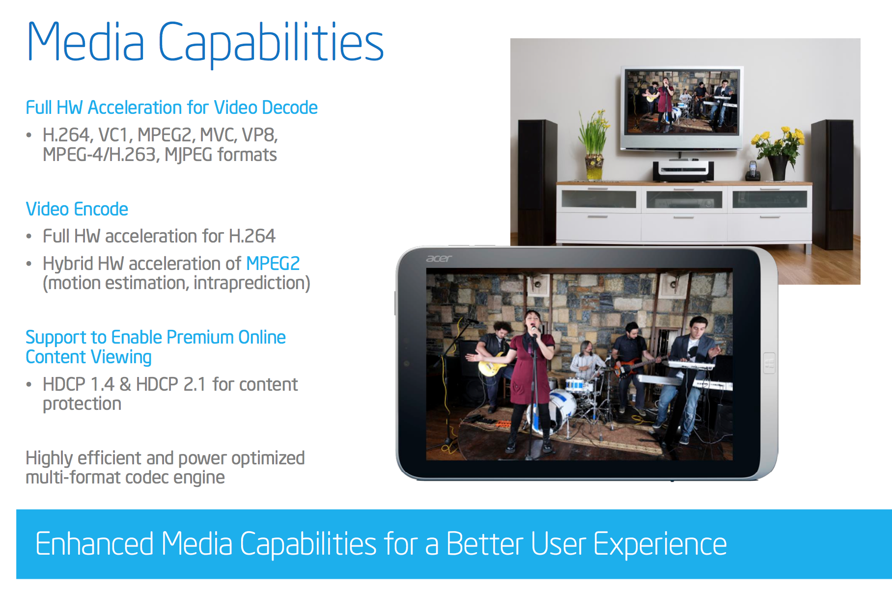
Video encode and decode blocks also shifted away from Imagination in Bay Trail. Both IP blocks are custom from Intel now. The ISP (Image Signal Processor) is from Silicon Hive (an Intel acquisition).


190 Comments
View All Comments
ancientarcher - Friday, September 13, 2013 - link
well, there are two different things here1) whether it costs less vs clovertrail or is it just that the pricing is different: Clovertrail was on the 32nm fab, which is 4-6 years old by now, whereas 22nm trigate is only 2 years old. Apart from the age of the fab, double patterning matters - it means that you have double the number of steps as single patterning (in same stages). Even for relatively old fabs, double patterning will increase costs. Trigate also adds cost, not least in testing. I would bet my last penny that Baytrail is more expensive to manufacture than clovertrail, but Intel is pricing it lower (meaning lower margin) to not repeat past mistakes. Pricing Baytrail at $100+ will mean missing the market altogether, no matter how good the chip is.
&
2) costs versus the core series is irrelevant. The final costs depend primarily on the area of the chip. But Intel hasn't given out any details. WHY??? might I ask. Given the amount of graphics power and cores (4 vs 2 in clovertrail), I would think that the area of the Baytrail might be closer to 100mm^2. So, yea the core i7 processor of 177mm^2 is much larger but sells for $450 retail. Big difference...
By the time Intel is readying to put these in a smartphone, Qualcomm and the others will have products in 20nm (planar) with at least ~30% increase to CPU and GPU (maybe more in GPU on HSA capability) and Intel will fall behind again.
FAIL!!
zeo - Saturday, September 14, 2013 - link
Sorry but you lose the cost bet, for one thing you're forgetting the 22nm FAB reduces the amount of material needed for each chip and they can put more units on each wafer! So mass produced the cost of things like Tri-Gate get absorbed and negated... The increase in cost is also less now than when they first introduced the 22nm FAB. This isn't new technology anymore and the FAB yields are high enough to reduce costs now!Simple fact of the matter is we're already seeing pricing announced for Bay Trail based devices and they're starting well below what Clover Trail devices were introduced at!
The Asus T100 only has a starting price of $349, PCMag even did a benchmark (something to do with matching names and addresses using an algorithm), which took Clover Trail over 30 minutes but the Z3740 in the T100 finished it in just over 15 Minutes... and it includes the Keyboard dock in the pricing!
So the lower pricing and higher performance is a reality!
And no, Intel will already be putting these in Smart Phones by the time Qualcomm and others will have products in 20nm in actual products! Merrifield is getting a early 2014 release and besides, by the time they do push out 20nm into actual products Intel will already be getting ready to push out their 14nm Airmont update, which they already put on a accelerated schedule for rollout!
Really, it's understandable to be pessimistic, Intel took over 5 years to get serious with both mobile and the ATOM but believe it or not they're finally serious about it...
ollienightly - Sunday, September 15, 2013 - link
This is just silly. Intel already put almost twice as much transistors as CT+ in BT-T. The die size should be similar, thus invalidate your whole point of being cheaper. 32nm was back then much older tech than 22nm now. 32nm began shipping back in Q4 2009, CT was some 3-years later. Assuming BT-T ships this year, there's only a 2-year gap since intel's first 22nm offerings. So neither die size nor maturity is on BT-T's side. And the sheer cost in moving to 22nm will be the deciding factor. I wouldn't be surprised if the silicon costs twice as much to make and the total cost is 30% higher.Pricing has NOTHING to do with cost itself. BT-T is priced lower to remain competitive, that's all. Case in point, Haswell 4C-GT2 (177mm2, 4702M@2.2GHz) is more expensive than Haswell 2C-GT3 (181mm2, 4600M@2.9GHz), that is with the same process, TDP, time to market. And higher frequency / bigger die has higher defection rate. So there goes your cost theory.
zeo - Sunday, September 15, 2013 - link
Ship this year?Really? Toshiba, Dell and Asus are shipping Bay Trail based products in just over a month and you're still on whether they'll ship this year!
ollienightly - Sunday, September 15, 2013 - link
Also, keep in mind NVIDIA claims the per transistor cost stopped being competitive beyond 28nm-node. The general trend holds true for Intel. Even more so in CT v BT-T case since 22nm is still young whereas when CT announced, 32nm HKMG was widely used by every FAB in the world.zeo - Sunday, September 15, 2013 - link
Nonsense, first 22nm was started longer than 2 years ago. It only began producing shipping products 2 years ago but they were working on the technology much longer than that and it doesn't take long to perfect, which they have to do before they seriously move on to the next FAB advancement and they're already starting to get ready for that as well!Really, Intel is way ahead on many of these technologies. For example, Intel had been using HKMG at 45nm, long before ARM manufacturers caught up at 32nm, and Tri-Gate is already a well developed technology for Intel. Also, Bay Trail is a much simpler chip than the Core Processors. So it's doesn't require as high precision to make as the much more complex Core processors and thus they are a lot easier to get good yields for them!
And again, my point is the prices of actual devices coming out with Bay Trail is lower than the previous Clover Trail... So regardless of what you think Bay Trail is in fact cheaper than Clover Trail!
Not to mention Intel stated this months ago that Bay Trail will be cheaper than Clover Trail! Actual product pricing shows they kept their word!
monstercameron - Friday, September 13, 2013 - link
wow, do some research dude, oems don't care about power, case-in-point acer w700 and all those other i3/i5 tablets [ivybridge]. The a4-5000 could fit in a tablet just as comfortably.Nagorak - Wednesday, September 11, 2013 - link
In that case, why not just hold out for a Haswell based tablet?lmcd - Wednesday, September 11, 2013 - link
I still wonder what the picture would be like with comparable graphics. Too bad the wait still isn't over. And imagine what happens when Jaguar hits the HPL process Qualcomm got access to.Homeles - Wednesday, September 11, 2013 - link
Jaguar is on GloFo. Snapdragon 800 is on TSMC.