Intel’s Silvermont Architecture Revealed: Getting Serious About Mobile
by Anand Lal Shimpi on May 6, 2013 1:00 PM EST- Posted in
- CPUs
- Intel
- Silvermont
- SoCs
The most frustrating part about covering Intel’s journey into mobile over the past five years is just how long it’s taken to get here. The CPU cores used in Medfield, Clover Trail and Clover Trail+ are very similar to what Intel had with the first Atom in 2008. Obviously we’re dealing with higher levels of integration and tweaks for further power consumption, but the architecture and much of the core remains unchanged. Just consider what that means. A single Bonnell core, designed in 2004, released in 2008, is already faster than ARM’s Cortex A9. Intel had this architecture for five years now and from the market’s perspective, did absolutely nothing with it. You could argue that the part wasn’t really ready until Intel had its 32nm process, so perhaps we’ve only wasted 3 years (Intel debuted its 32nm process in 2010). It’s beyond frustrating to think about just how competitive Intel would have been had it aggressively pursued this market.
Today Intel is in a different position. After acquisitions, new hires and some significant internal organizational changes, Intel seems to finally have the foundation to iterate and innovate in mobile. Although Bonnell (the first Atom core) was the beginning of Intel’s journey into mobile, it’s Silvermont - Intel’s first new Atom microarchitecture since 2008 - that finally puts Intel on the right course.
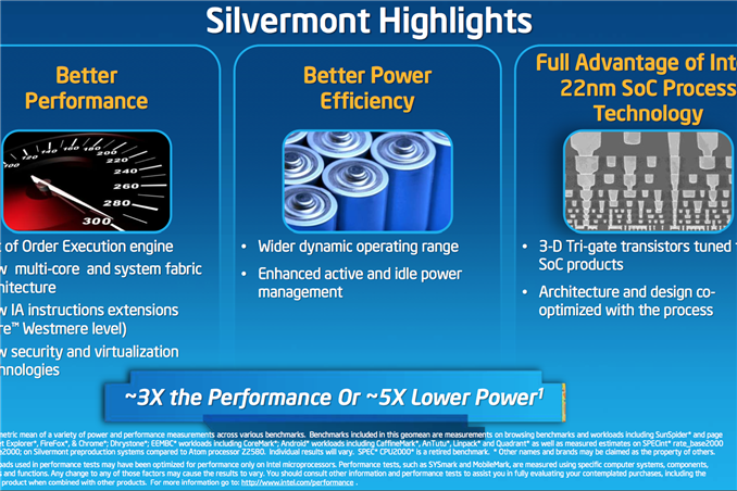
Although Silvermont can find its way into everything from cars to servers, the architecture is primarily optimized for use in smartphones and then in tablets, in that order. This is a significant departure from the previous Bonnell core that was first designed to serve the now defunct Mobile Internet Devices category that Intel put so much faith in back in the early to mid 2000s. As Intel’s first Atom architecture designed for mobile, expectations are high for Silvermont. While we’ll have to wait until the end of the year to see Silvermont in tablets (and early next year for phones), the good news for Intel is that Silvermont seems competitive right out of the gate. The even better news is that Silvermont will only be with us for a year before it gets its first update: Airmont.
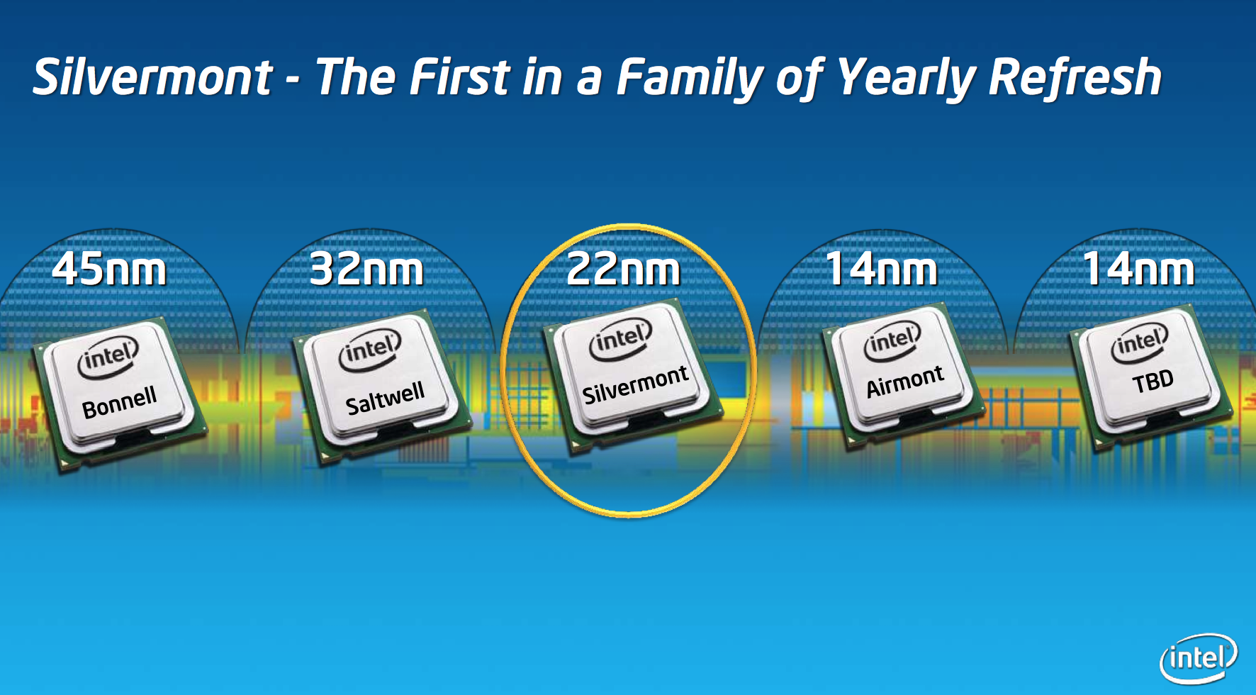 Intel made this announcement last year, but Silvermont is the beginning of Intel’s tick-tock cadence for Atom. Intel plans on revving Atom yearly for at least the next three years. Silvermont introduces a new architecture, while Airmont will take that architecture and bring it down to 14nm in 2014/2015. One year later, we’ll see another brand new architecture take the stage also on 14nm. This is a shift that Intel needed to implement years ago, but it’s still not too late.
Before we get into an architectural analysis of Silvermont, it’s important to get some codenames in order. Bonnell was the name of the original 45nm Atom core, it was later shrunk to 32nm and called Saltwell when it arrived in smartphones and tablets last year. Silvermont is the name of the CPU core alone, but when it shows up in tablets later this year it will do so as a part of the Baytrail SoC and a part of the Merrifield SoC next year in smartphones.
22nm
To really understand the Silvermont story, you need to first understand Intel’s 22nm SoC process. Two years ago Intel announced its 22nm tri-gate 3D transistors, which would eventually ship a year later in Intel’s Ivy Bridge processors. That process wasn’t suited for ultra mobile. It was optimized for the sort of high performance silicon that was deployed on it, but not the ultra compact, very affordable, low power silicon necessary in smartphones and tablets. A derivative of that process would be needed for mobile. Intel now makes two versions of all of its processes, one optimized for its high performance CPUs and one for low power SoCs. P1270 was the 22nm CPU process, and P1271 is the low power SoC version. Silvermont uses P1271. The high level characteristics are the same however. Intel’s 22nm process moves to tri-gate non-planar transistors that can significantly increase transistor performance and/or decrease power.

This part is huge. The move to 22nm 3D transistors lets Intel drop threshold voltage by approximately 100mV at the same leakage level. Remember that power scales with the square of voltage, so a 100mV savings depending on what voltage you’re talking about can be very huge. Intel’s numbers put the power savings at anywhere from 25 - 35% at threshold voltage. The gains don’t stop there either. At 1V, Intel’s 22nm process gives it an 18% improvement in transistor performance or at the same performance Intel can run the transistors at 0.8V - a 20% power savings. The benefits are even more pronounced at lower voltages: 37% faster performance at 0.7V or less than half the active power at the same performance.
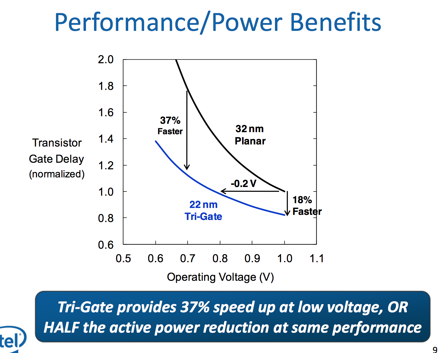
The end result here is Intel can scale frequency and/or add more active logic without drawing any more power than it did at 32nm. This helps at the top end with performance, but the vast majority of the time mobile devices are operating at very lower performance and power levels. Where performance doesn’t matter as much, Intel’s 22nm process gives it an insane advantage.
If we look back at our first x86 vs. ARM performance data we get a good indication of where Intel’s 32nm process had issues and where we should see tangible improvements with the move to 22nm:
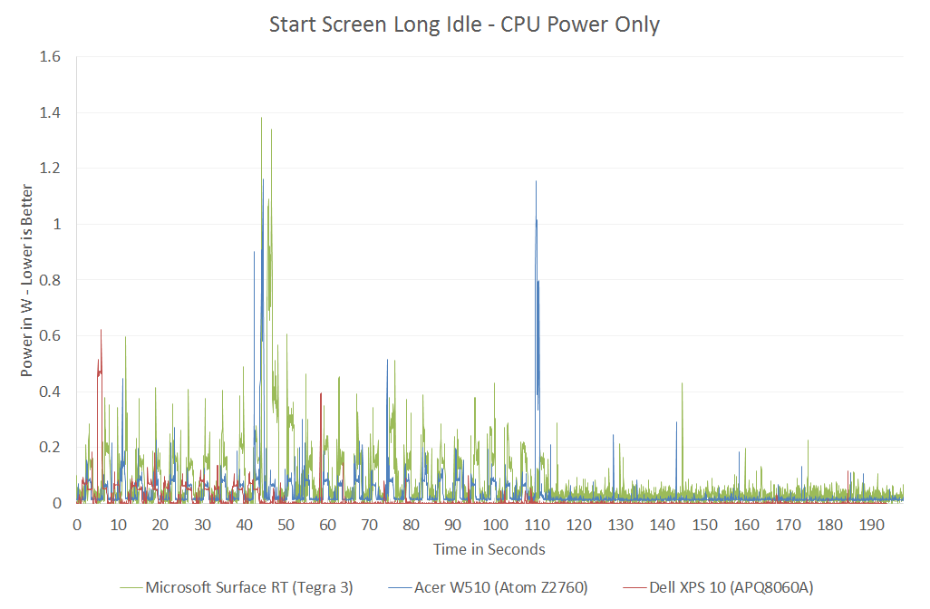
Qualcomm’s 28nm Krait 200 was actually able to get down to lower power levels than Intel could at 32nm. Without having specific data I can’t say for certain, but it’s extremely likely that with Silvermont Intel will be able to drive down to far lower power levels than anything we’ve ever measured.
Understanding what Intel’s 22nm process gives it is really key to understanding Silvermont.


174 Comments
View All Comments
silverblue - Monday, May 6, 2013 - link
I do wonder how much having a dual channel memory interface helps Silvermont, though. It's something that neither Atom nor Bobcat has enjoyed previously, and I've not heard much about Jaguar on this subject (ignoring the PS4, that is). AMD certainly has the lead on ISAs though, so regardless of how good Silvermont is, it's going to trail in some places.I'm a little confused as to the virtual lack of a comparison to AMD in this piece; yes, Intel did say they wanted to beat ARM at its own game, but with Jaguar-powered devices already in the wild and AMD sporting a new custom-CPU team for whoever wants whatever, this is going to be interesting.
Benchmarks, please! ;)
powerarmour - Monday, May 6, 2013 - link
Atom had dual channel memory with the ION chipset btw.silverblue - Monday, May 6, 2013 - link
Really? Oh well, in that case then, maybe not too much.Spunjji - Wednesday, May 8, 2013 - link
Only until Intel murdered that, of course :|ajp_anton - Monday, May 6, 2013 - link
Where did you find "8x" in the slides?Gigaplex - Tuesday, May 7, 2013 - link
AMDs HSA is most definitely something to be enthusiastic about.theos83 - Monday, May 6, 2013 - link
You're right, I've seen this tendency in AT's reviews and discussions as well. I understand that a lot of it comes from reviewing PC components and processors where Intel dominated the market. Also, most of the slides here are marketing material. For example, the 22nm Ivy Bridge tri-gate plots have been out since 2011. True, Intel is the first and only foundry to bring FinFETs to the market successfully and I applaud them for that. However, the performance vs power advantage is not that evident, since even though Tri-gates allow 100mV reduction in threshold voltage and hence, supply voltage, various blogs have reported that most Ivy bridge processors did not scale down supply voltage below 0.9V. FinFETs are great for high performance parts, however, you need to really pay attention to reliability and variation to make it successful for SoCs, they are a completely different ball-game.Also, the rest of the SoC makers already have roadmaps ready for the future, they are a fast moving target. Hence lets see benchmarked numbers from Intel processors before jumping on the marketing bandwagon.
Pheesh - Monday, May 6, 2013 - link
"However, the performance vs power advantage is not that evident, since even though Tri-gates allow 100mV reduction in threshold voltage and hence, supply voltage, various blogs have reported that most Ivy bridge processors did not scale down supply voltage below 0.9V." Didn't the start of the article cover that they are using a different manufacturing process for these lower power SOC's as compared to ivy bridge processors?saurabhr8here - Monday, May 6, 2013 - link
The SoC process has some differences in the metal stack for higher density and has additional transistor flavors (longer channel lengths). Check Intel's IEDM 2012 paper for more information, however, the truth is that their tri-gate process improvements claimed in the 'plots' shown and actual performance improvements in processors have a significant gap. I think that Intel tri-gates are great, but they aren't as 'wonderful' as presented in the marketing slides.Krysto - Monday, May 6, 2013 - link
Thank You! People are starting to get it.