The Xeon Phi at work at TACC
by Johan De Gelas on November 14, 2012 1:44 PM EST- Posted in
- Cloud Computing
- CPUs
- IT Computing
- Intel
- Larrabee
- Xeon
- Xeon Phi
The Xeon Phi family of co-processors was announced in June, but Intel finally disclosed additional details.The Xeon Phi die is a massive chip: Almost 5 billion transistors using Intel's most advanced 22nm process technology with 3D tri-gate transistors.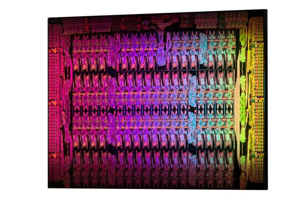
A maximum of 62 cores can fit on a single die. Each core is a simple in order x86 CPU (derived from the original Pentium) with a 512-bit SIMD unit. There is a twist though: the core can handle 4 threads simultaneously. Nehalem, Sandy and Ivy Bridge also use SMT, but those cores uses SMT mostly to make better use of their ample execution resources.
In case of the Xeon Phi core, the 4 threads are mostly a way to hide memory latency. In the best case, two threads will execute in parallel.
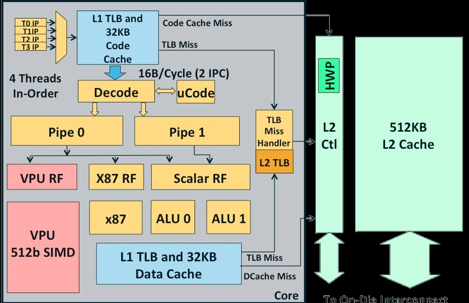
Each of these cores is a 64-bit x86 core. However, only 2% of the core logic (excluding the L2-cache) is spent on x86 logic. The SIMD unit does not support MMX, SSE or AVX: the Xeon Phi has its own vector format.
All of the cores are connected together with a bi-directional ring, similar to what's used in the Xeon E7 and the Sandy Bridge EP CPUs.
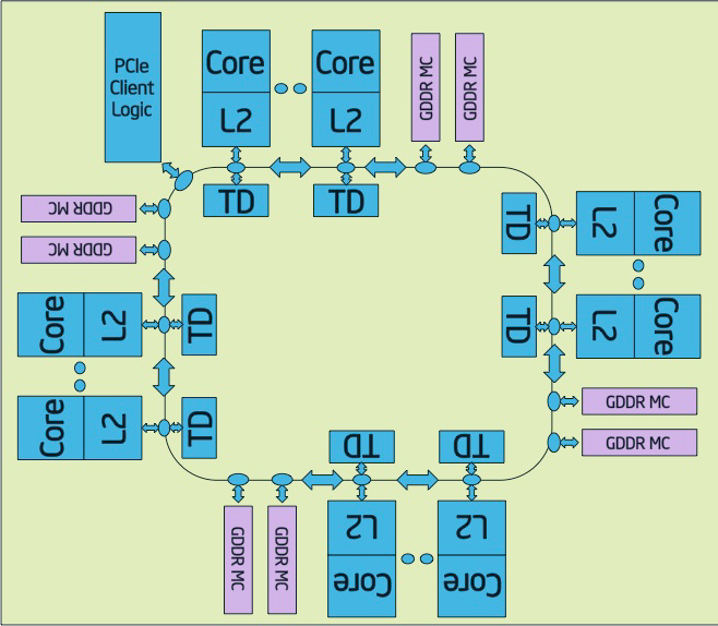
Eight memory channels (512-bit interface) support up to 8 GB of RAM, and PCIe logic is on chip.


46 Comments
View All Comments
creed3020 - Friday, November 16, 2012 - link
There are only 4 per row in the chassis because these units in Stampede feature the Xeon Phi card which requires a bigger sled. The author got the potential specs messed up with the way they are actually configured for this supercomputer.GullLars - Thursday, November 15, 2012 - link
So, it seems these are great at general purpose supercomputing.How do they stack up against the latest FPGAs if they are set up carefully by the people who will be running a specialized problem on them?
And would these be able to work effectively with offloading of some key functions that would be able to work 20-100x faster (or power efficient) on a carefully set up FPGA?
Some people in the comments mentioned hetrogenous computing. A step on the way is modular accelerated code. I'm interrested to see if we get more specialized hardware for acceleration in the comming years, not just graphics (with transcoding) and encryption/decryption like is common in CPUs now. Or if we get an FPGA component (integrated or PCIe) that can be reserved and set up by programs to realize huge speedups or power savings.
Jameshobbs - Monday, November 19, 2012 - link
Why have there not been a lot of reports regarding the PCI express. This was the first source that I was able to find that even mentions the speed of the PCI e bus for the Xeon Phi.One of the most challenging things for programming on accelerators is handling the PCI express and trying to balance data transfer with computational complexity. Everyone, NVIDIA, Intel, AMD seem to be doing a lot of arm waving regarding this issue, and there are many GPU papers that tend to omit the transfer times in their results. To me I find this dishonest and cheating.
One thing that continues to shock me as well is that people keep complaining about how difficult it is to debug a GPU program and then they reference old out of date references such as http://lenam701.blogspot.be/2012/02/nvidia-cuda-my... which was mentioned above. The things that the author of that blog post complained about have been resolved in the latest versions of CUDA (from 4.2 onward... maybe even in 4.0).
Programmers can now use printf and it is possible to hook a debugger into a GPU application to do more in depth debugging. The main thing that bothers me about GPU programming is you must check to make sure a program has successfully completed or not. Other than that I find it relatively easy to debug a GPU application.
MySchizoBuddy - Wednesday, November 21, 2012 - link
Next version of AMD APU will allow both the GPU and CPU access to the same memory locations.sheepdestroyer - Wednesday, December 5, 2012 - link
i would really like to see a benchmark of this cpu on LLVMpipehttp://www.mesa3d.org/llvmpipe.html
The original Larabee would have had a DirectX translation layer and this project could be seen as an OpenGL version of it.
Just loading a distro with Gnome 3 running on LLVMpipe or benchmarking some ioq3 and iodoom3 games would be VERY interesting.
tuklap - Sunday, March 3, 2013 - link
Can this accelerate my normal PC applications like Rendering in AutoCAD/Revit, Media Conversion, STAAD, ETABS and etc computations???or do i Have to create my own applications?