SK Hynix Announces Its First HBM3 Memory: 24GB Stacks, Clocked at up to 6.4Gbps
by Ryan Smith on October 20, 2021 9:30 AM EST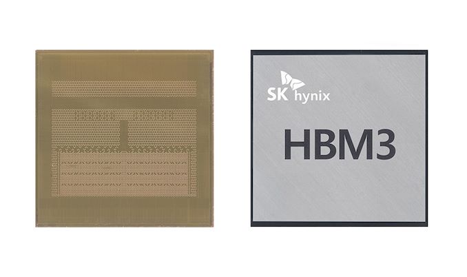
Though the formal specification has yet to be ratified by JEDEC, the memory industry as a whole is already gearing up for the upcoming launch of the next generation of High Bandwidth Memory, HBM3. Following announcements earlier this summer from controller IP vendors like Synopsys and Rambus, this morning SK Hynix is announcing that it has finished development of its HBM3 memory technology – and according to the company, becoming the first memory vendor to do so. With controller IP and now the memory itself nearing or at completion, the stage is being set for formal ratification of the standard, and eventually for HBM3-equipped devices to start rolling out later in 2022.
Overall, the relatively lightweight press release from SK Hynix is roughly equal parts technical details and boasting. While there are only 3 memory vendors producing HJBM – Samsung, SK Hynix, and Micron – it’s still a technically competitive field due to the challenges involved in making deep-stacked and TSV-connected high-speed memory work, and thus there’s a fair bit of pride in being first. At the same time, HBM commands significant price premiums even with its high production costs, so memory vendors are also eager to be first to market to cash in on their technologies.
In any case, both IP and memory vendors have taken to announcing some of their HBM wares even before the relevant specifications have been announced. We saw both parties get an early start with HBM2E, and now once again with HBM3. This leaves some of the details of HBM3 shrouded in a bit of mystery – mainly that we don’t know what the final, official bandwidth rates are going to be – but announcements like SK Hynix’s help narrow things down. Still, these sorts of early announcements should be taken with a small grain of salt, as memory vendors are fond of quoting in-lab data rates that may be faster than what the spec itself defines (e.g. SK Hynix’s HBM2E).
Getting into the technical details, according to SK Hynix their HBM3 memory will be able to run as fast as 6.4Gbps/pin. This would be double the data rate of today’s HBM2E, which formally tops out at 3.2Gbps/pin, or 78% faster than the company's off-spec 3.6Gbps/pin HBM2E SKUs. SK Hynix’s announcement also indirectly confirms that the basic bus widths for HBM3 remain unchanged, meaning that a single stack of memory is 1024-bits wide. At Hynix’s claimed data rates, this means a single stack of HBM3 will be able to deliver 819GB/second worth of memory bandwidth.
| SK Hynix HBM Memory Comparison | |||||
| HBM3 | HBM2E | HBM2 | |||
| Max Capacity | 24 GB | 16 GB | 8 GB | ||
| Max Bandwidth Per Pin | 6.4 Gb/s | 3.6 Gb/s | 2.0 Gb/s | ||
| Number of DRAM ICs per Stack | 12 | 8 | 8 | ||
| Effective Bus Width | 1024-bit | ||||
| Voltage | ? | 1.2 V | 1.2 V | ||
| Bandwidth per Stack | 819.2 GB/s | 460.8 GB/s | 256 GB/s | ||
SK Hynix will be offering their memory in two capacities: 16GB and 24GB. This aligns with 8-Hi and 12-Hi stacks respectively, and means that at least for SK Hynix, their first generation of HBM3 memory is still the same density as their latest-generation HBM2E memory. This means that device vendors looking to increase their total memory capacities for their next-generation parts (e.g. AMD and NVIDIA) will need to use memory with 12 dies/layers, up from the 8 layer stacks they typically use today.
What will be interesting to see in the final version of the HBM3 specification is whether JEDEC sets any height limits for 12-Hi stacks of HBM3. The group punted on the matter with HBM2E, where 8-Hi stacks had a maximum height but 12-Hi stacks did not. That in turn impeded the adoption of 12-Hi stacked HBM2E, since it wasn’t guaranteed to fit in the same space as 8-Hi stacks – or indeed any common size at all.
On that matter, the SK Hynix press release notably calls out the efforts the company put into minimizing the size of their 12-Hi (24GB) HBM3 stacks. According to the company, the dies used in a 12-Hi stack – and apparently just the 12-Hi stack – have been ground to a thickness of just 30 micrometers, minimizing their thickness and allowing SK Hynix to properly place them within the sizable stack. Minimizing stack height is beneficial regardless of standards, but if this means that HBM3 will require 12-Hi stacks to be shorter – and ideally, the same height as 8-Hi stacks for physical compatibility purposes – then all the better for customers, who would be able to more easily offer products with multiple memory capacities.
Past that, the press release also confirms that one of HBM’s core features, integrated ECC support, will be returning. The standard has offered ECC since the very beginning, allowing device manufacturers to get ECC memory “for free”, as opposed to having to lay down extra chips with (G)DDR or using soft-ECC methods.
Finally, it looks like SK Hynix will be going after the same general customer base for HBM3 as they already are for HBM2E. That is to say high-end server products, where the additional bandwidth of HBM3 is essential, as is the density. HBM has of course made a name for itself in server GPUs such as NVIDIA’s A100 and AMD’s M100, but it’s also frequently tapped for high-end machine learning accelerators, and even networking gear.
We’ll have more on this story in the near future once JEDEC formally approves the HBM3 standard. In the meantime, it’s sounding like the first HBM3 products should begin landing in customers’ hands in the later part of next year.
Source: SK Hynix


19 Comments
View All Comments
lemurbutton - Wednesday, October 20, 2021 - link
Nice. Might go into the upcoming Mac Pro 40 CPU core / 128 GPU core monster SoC.web2dot0 - Wednesday, October 20, 2021 - link
Guarantee it will ... 8/16Channel HBM3 ...sonny73n - Thursday, October 21, 2021 - link
Keep dreaming, sheeple!GC2:CS - Wednesday, October 20, 2021 - link
I do not think Apple is even considering HBM at all. They just want to go for some absurd lenghts and lengths with standard memory and use it for GPU as well. They will just scale up what hey have with the A14. At premium that is to be said.Also when we will see some HBM in phones ? Like a 256 bit interface tsv-ed directly to the SoC ?
That would be probably a big benefit from efficiency standpoint
Diogene7 - Wednesday, October 20, 2021 - link
@GC2:CS: I am wondering the same thing about smartphones :1. Would there be any significant power efficiency advantages using HBM memory in a smartphone ?
2. I would dream to have persistent memory like SOT-MRAM used in HBM memory stack used in a smartphone and Internet of Things (IoT) objects : it would provide a large fast memory that is non-volatile, it would clearly unlock new and tremendously improved user experiences !!!
Ex: smartphone with low power 128GB of HBM non volatile memory : no lpddr DRAM, neither flash storage…
DanNeely - Wednesday, October 20, 2021 - link
IIRC HBM is significantly higher in power than standard DDR memory. It's better than GDDR; but that's a relatively low bar for power efficiency.TanjB - Wednesday, October 20, 2021 - link
HBM is about 10x more efficient per bit transferred than DDR. Varying by vendor and by chip, but roughly 4 pJ/bit for HBM2e vs. 40 pJ/bit for DDR4 or 5. HBM3 might be a bit higher energy than 2e due to the higher transfer rate: we will need to see the data sheets. But no way it is as inefficient as DDR4 or 5.Even if you measure by capacity rather than by activity it is not clear which would win. Internally they use pretty much the same DRAM technology, and if they are not in use the interfaces idle very efficiently, so they probably have roughly the same idle power per GB. Overall, HBM is more efficient when it comes to getting work done, much more efficient.
Samus - Thursday, October 21, 2021 - link
Even RDRAM had power efficiency gains over SDRAM\DDR at the time, but it was down to power states. At full throttle, RAMBUS (and HBMx) will use more power but as TanjB said, at full power it is provides so much more bandwidth that the power efficiency is much better. It just isn't designed for power-sensitive applications.BUT it could be. If the power states were tweaked and throttled, it could theoretically provide more bandwidth per watt than DDR and especially GDDR while probably undercutting the cost of GDDR assuming the memory controller is a cost-effective implementation (that's a rabbit hole I'm not jumping into - memory controller implementations are an even more complex topic, just ask AMD why their Ryzen architecture is so picky about memory latency, especially ranking)
Wereweeb - Wednesday, October 20, 2021 - link
Yes, HBM uses less power for an equivalent amount of non-HBM bandwidth. However, a single stack of HBM3 will deliver around 800GB/s. Four 16-bit channels of LPDDR5 deliver up to 51GB/s. Smartphones simply don't need HBM levels of bandwidth.Maybe in the future, when they develop low-cost HBM, and if manufacturers chipletize smartphone SoC's, it might make sense to just put everything on the same interposer (I.e., to use HBM). Today's not that day.
As for MRAM: it isn't and won't be cost-competitive with current planar DRAM for *at the very least* a decade, and if we get 3D-DRAM and/or capacitorless DRAM, you can pretty much forget it.
8GB of SOT-MRAM would already be prohibitively expensive, 128GB would only be in a consumer product for a Saudi oil prince. (It would cost me 154k USD from Mouser, disregarding the probable bulk discount)
Don't get me wrong, MRAM is very interesting, maybe even close to a theoretically "perfect memory", but today it is better as a replacement for embedded SRAM, NOR flash, etc... (Where you only need 1MB of it anyway) and, in one or two decades, possibly replace L3 SRAM caches. It's otherwise simply too large/too complex of a cell (read: very costly) to be used as a main memory, not to speak of storage.
I'm more interested in seeing capacitorless DRAM, 3D DRAM, 3D PCM, and in a few years maybe some non-Intel competitor to Optane based on something like CeRAM, that is promised to be easier to manufacture. But the other technologies will come at most as a complement to DRAM for at least two more decades, partly thanks to the fact that real R&D (The lengthy work of material and process optimization) is tied down in what makes companies money in the short term. And I doubt anything is replacing NAND in the next decades.
TanjB - Wednesday, October 20, 2021 - link
Not all ECC is the same. It appears the built-in ECC is just SEC, same as in LPDDR5 and DDR5 chips, which can only correct single bits and cannot report when errors are not corrected. The industry does not publish data on expected error rates of their chips so we have to guess: it might be reasonable to guess that is 90% of the actual errors.This work shows that additional, external ECC will still be needed to get high reliability with HBM3:
https://ieeexplore.ieee.org/abstract/document/9556...