Intel's Process Roadmap to 2025: with 4nm, 3nm, 20A and 18A?!
by Dr. Ian Cutress on July 26, 2021 5:00 PM ESTNew Technology Features for 2024: RibbonFETs
One of the major features of this roadmap is highlighted when it shifts to 20A, Intel’s process name referring to Angstroms rather than nanometers. At this juncture, as mentioned above, Intel will be transitioning from its FinFET design over to a new type of transistor, known as a Gate-All-Around transistor, or GAAFET. In Intel’s case, the marketing name they are giving their version is RibbonFET.
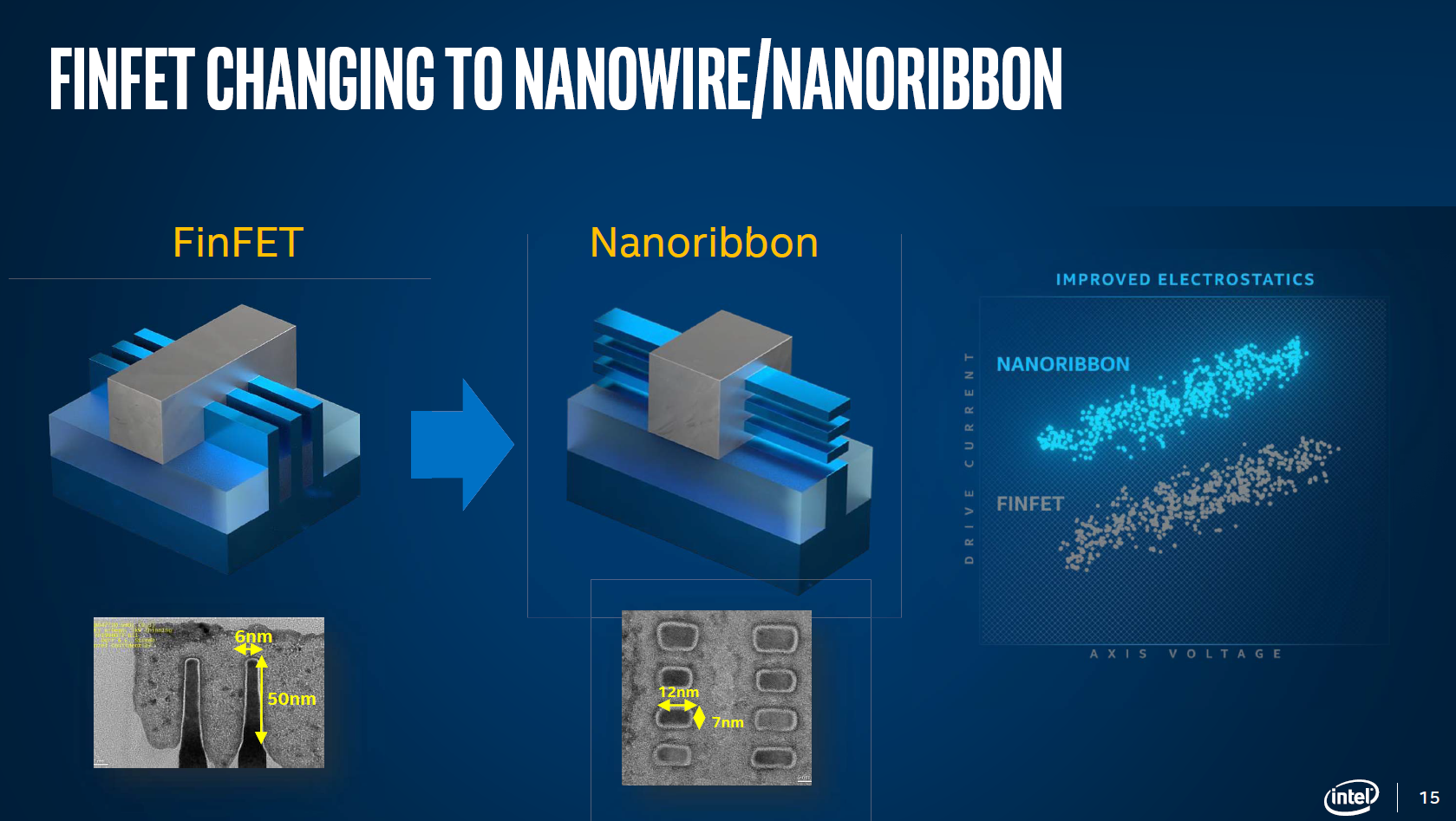
It has been widely expected that once the standard FinFET runs out of steam that the semiconductor manufacturing industry will pivot to GAAFET designs. Each of the leading edge vendors call their implementation something different (RibbonFET, MBCFET), but it is all using the same basic principle – a flexible width transistor with a number of layers helping drive transistor current. Where FinFETs relies on multiple quantized fins for source/drain and a cell height of multiple tracks of fins, GAAFETs enable a single fin of variable length, allowing the current for each individual cell device to be optimized in power, performance, or area.
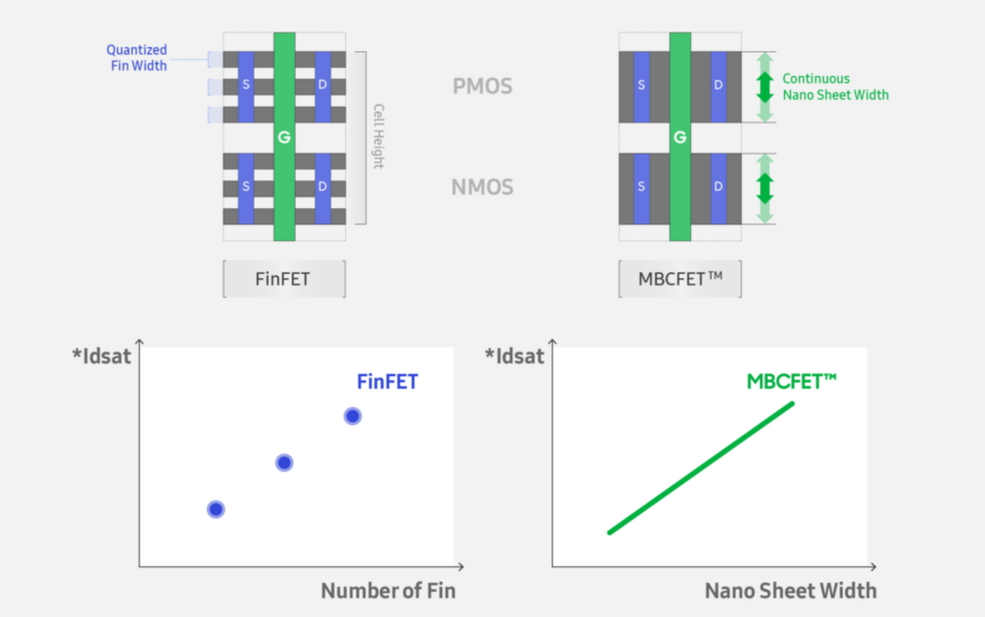
Image from Samsung
Intel has been discussing GAAFETs in technical semiconductor conferences for a number of years, at the International VLSI conference in June 2020, then CTO Dr. Mike Mayberry showcased a diagram with the enhanced electrostatics of moving to a GAA design. At the time we asked about Intel’s timescale for implementing GAA in volume, and were told to expect them ‘within 5 years’. At present Intel’s RibbonFET is due to come with the 20A process, likely to be productized by the end of 2024 based on the roadmaps outlined above.
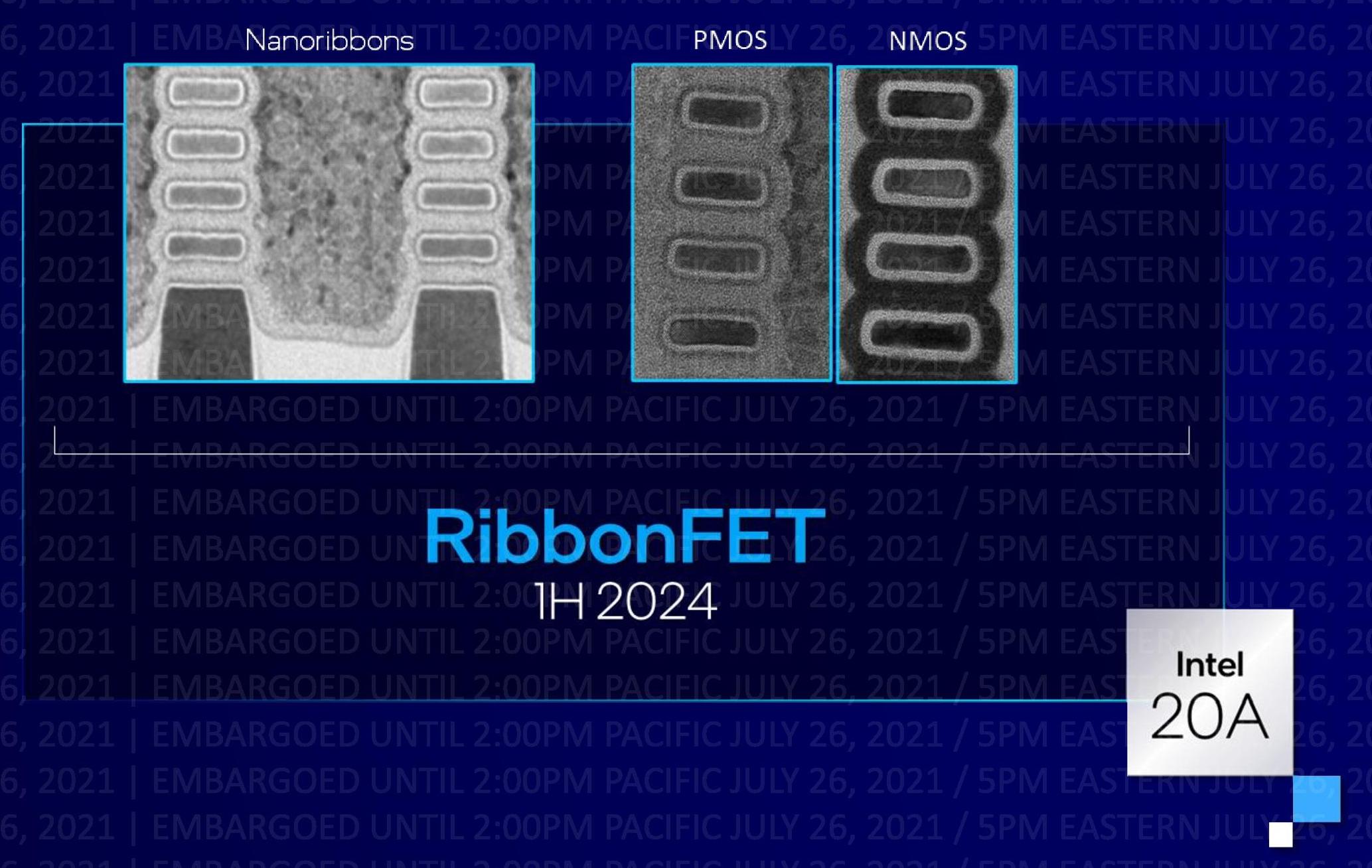
In Intel’s RibbonFET diagrams for this event, they’re showing both PMOS and NMOS devices, as well as what clearly looks like a 4-stack design. Given that I have seen presentations from Intel involving anything from 2-stack to 5-stack at the industry conferences, we confirmed that Intel will indeed be using a 4-stack implementation. The more stacks that are added, the more process node steps are required for manufacturing, and to quote Intel’s Dr. Kelleher, ‘it’s easier to remove a stack than to add one!’. Exactly what is the right number of stacks for any given process or function is still an active area of research, however Intel seems keen on four.
In comparison with Intel’s competitors,
TSMC is expected to transition to GAAFET designs on its 2nm process. At its annual Tech Symposium in August 2020, TSMC confirmed that it would remain on FinFET technology all the way to its 3nm (or N3) process node as it has been able to find significant updates to the technology to allow performance and leakage scaling beyond what was initially expected – N3 is quoted to have up to a 50% performance gain, 30% power reduction, or 1.7x density gain over TSMC N5. Staying on FinFETs, TSMC stated, provides comfort to its customers. Details on TSMC’s N2 have not been disclosed.
Samsung by contrast has stated that it will be introducing its GAA technology with its 3nm process node. Back in Q2 2019, Samsung Foundry announced the first v0.1 development kit of its new 3GAE process node using GAAFETs was being made available to key customers. At the time Samsung predicted volume production by end of 2021, and the latest announcement suggests that while 3GAE will deploy in 2022 internally, main customers may have to wait until 2023 for its more advanced 3GAP process.
To put this into a table:
| Gate-All-Around Transistor Deployment | |||
| AnandTech | Name | Process | Timeframe |
| Intel | RibbonFET | 20A | 2024 |
| 18A | 2025 | ||
| TSMC | GAAFET | N2 / 2nm | EoY 2023? |
| Samsung | MBCFET | 3GAE | 2022 |
| 3GAP | 2023 | ||
By this metric, Samsung might be first to the gate, albeit with an internal node, while TSMC is going to get a lot out of its N5, N4, and N3 nodes first. Around end of year 2023 is when it gets interesting as TSMC may be looking at its N2 designs, while Intel is committed to that 2024 timeframe. The official slide says first half 2024, though as a technology announcement vs product announcement, there is often some lag between the two.
New Technology Features for 2024: PowerVias
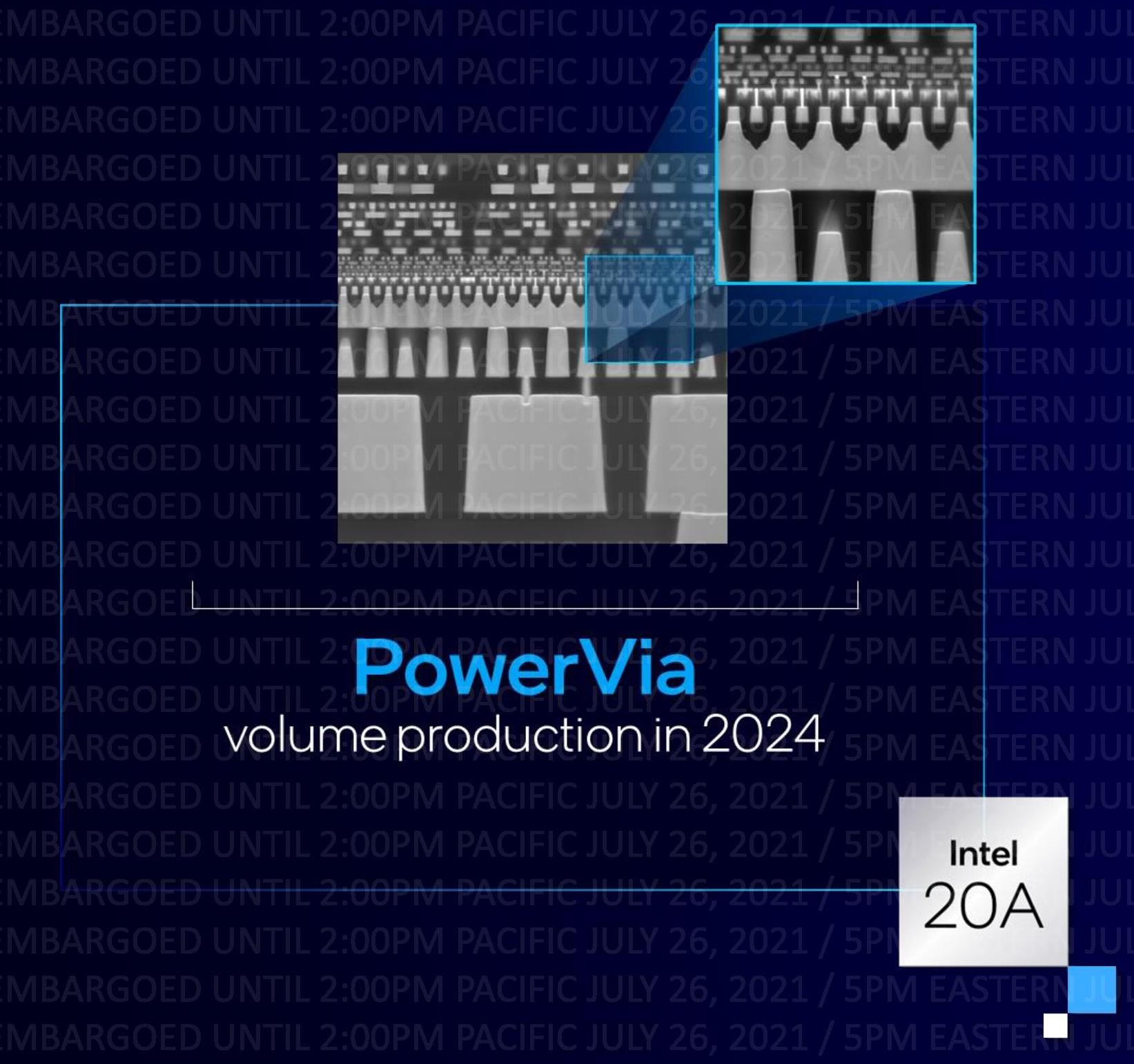
The other arm of Intel’s 20A designs in 2024 is what the company is calling ‘PowerVia’. The concept here pivots the traditional understanding of chip design from a multi-layered cake into a sandwich of sorts.
The manufacturing process of a modern circuit starts the transistor layer, M0, as the smallest layer. Above that, additional metal layers are added at increasing sizes to account for all the wiring needed between the transistors and different parts of the processor (cache, buffers, accelerators). A modern high-performance processor typically has anywhere from 10 to 20 metal layers in its design, with the top layer where the external connections are placed. The chip is then flipped over (known as flip chip) so that the chip can talk to the outside world with those connections on the bottom, and the transistors at the top.
With PowerVias, we now put the transistors in the middle of the design. On one side of the transistors we put the communication wires that allow parts of the chip to talk to each other. On the other side are all the power related connections (along with power gating control). In essence, we moved to a sandwich where the transistors are the filling. This is usually referred to as ‘backside power delivery’ in the industry – PowerVia is Intel’s marketing name.
From a holistic level, we can ascertain that the benefits of this design start with simplifying both the power and the connectivity wires. Typically these have to be designed to ensure there is no signaling interference, and one of the big sources of interference are large power carrying wires, so this takes them out of the equation by putting them on the other side of the chip. It also works the other way – the interference of the interconnected data wires can increase the power delivery resistance, resulting in lost energy and thermals. In this way, PowerVias can help new generations of transistors as drive currents increase by having the power directly there, rather than routed around the connectivity.
There are a couple of hurdles here to mention however. Normally we start manufacturing the transistors first because they are the most difficult and most likely to have defects – if a defect is caught early in the metrology (defect detection in manufacturing), then that can be reported as early in the cycle as possible. By having the transistors in the middle, Intel would now be manufacturing several layers of power first before getting to the tough bit. Now technically these layers of power would be super easy compared to the transistors, and nothing is likely to go wrong, but it is something to consider.
The second hurdle to think about is power management and thermal conductivity. Modern chips are built transistor first into a dozen layers ending with power and connections, and then the chip is flipped, so the power hungry transistors are now at the top of the chip and the thermals can be managed. In a sandwich design, that thermal energy is going to go through whatever ends up on the top of the chip, which is most likely going to be the internal communication wires. Assuming that the thermal increase of these wires doesn’t cause any issues in production or regular use, then perhaps this isn’t so much of an issue, however it is something to consider when heat has to be conducted away from the transistors.
It is worth noting that this ‘backside power delivery’ technology has been in development for a number of years. Across five research papers presented at the VLSI symposium in 2021, imec presented several papers on the technology showing recent advancements when using FinFETs, and in 2019 Arm and imec announced similar technology on an Arm Cortex-A53 built on an equivalent 3nm process in imec’s research facilities. Overall the technology reduces the IR drop on the design, which is becoming increasingly harder to achieve on more advanced process node technologies to drive performance. It will be interesting to see the technology when it is in high volume on high performance processors.


326 Comments
View All Comments
JoeDuarte - Tuesday, August 3, 2021 - link
That's not how knowledge works, or how reality works. It's not possible to know the answers to these sorts of questions by a moment's reflection and opinion generation, especially when the opinions contain no real info. "smart enough to invest" is meaningless without concrete data, like how much "Taiwan" actually "invested" in TSMC, when they did so, and how this investment influenced TSMC's ability to develop new nodes, if at all.(And your second clause is probably false in that I don't think any chipmaker wastes all of their retained earnings on shareholders, and of course "wastes" is a loaded term that would have to be justified with arguments and data.)
You can't really know anything about the world around you using your method here.
mode_13h - Wednesday, August 4, 2021 - link
> You can't really know anything about the world around you using your method here.To put it another way: the term for inferencing without data is "imagination".
mode_13h - Tuesday, July 27, 2021 - link
> It would be very interesting to see some rigorous organizational research on> how some foundries are able to reliably advance with new nodes and shrinks
True. But these must be closely-held secrets. I'm sure they'd closely guard them for decades.
> it looks like Intel is simply unable to advance.
They're advancing, just slowly. They finally got 10 nm performing competitively, by the time they reached 10 nm++ (SuperFin).
And they've delivered products with Foveros and EMIB.
That's why I said above that it's not a question so much of *whether* Intel will deliver, but in what decade!
JoeDuarte - Monday, August 9, 2021 - link
Is Foveros in anything? In desktops? I haven't heard anything.I don't remember what EMIB is, but it only matters if it matters. That is, if it confers benefits to users, like speed.
I don't trust their plus sign stacking anymore, or labels like "Super"-this or that. At this point it's all going to be bottom line metrics for me re: Intel. Is it faster? How much faster? That sort of thing.
Also, it has to actually exist and be ready to buy by normal means, like Dell, Amazon, etc. If there are no desktops with SuperFin+++++ Tiger Claw, Cougar Lake, Bald Eagle Lake, Rocket Man, etc. then it's moot. I think whatever Lake is supposed to have SuperFin++++ is in desktops yet.
JoeDuarte - Monday, August 9, 2021 - link
I *don't* think...mode_13h - Tuesday, August 10, 2021 - link
> Is Foveros in anything? In desktops? I haven't heard anything.Lakefield, but I'm guessing that's why you added "in desktops". Chip development times seem to be around 4 years or so. That means you wouldn't expect an overnight transition to something like Foveros. First, it has to be proven and refined. Then, you might see chips still early in their design phase start to utilize it, but that should result in a gap between the first example and more widespread adoption. So, the fact that we haven't yet seen widespread adoption doesn't mean anything, in itself.
> I don't remember what EMIB is
It's easy to look up. It's Intel's technology for building multi-chip modules. I think Sapphire Rapids is slated to use it. Otherwise, I think Meteor Lake might be first.
> I don't trust their plus sign stacking anymore
If we were talking about 14 nm, then I'd agree. However, they've been a bit more transparent about what distinguishes 10 nm+, 10 nm++, and 10 nm+++. For details, see the article (which refers to ++ as SF and +++ as ESF).
> Is it faster? How much faster? That sort of thing.
Their foundry business should offer new transparency into their manufacturing node. Before, when Intel was practically their fabs' only customer, they didn't need to reveal detailed performance characteristics of their process iterations. However, when you're trying to attract customers to use your fabs, the standard for transparency is a lot higher. It also means that Intel needs to be more conservative about their roadmaps, since actual manufacturing contracts are going to hang by on-time and on-target delivery.
However, I agree that the end result (cost, area, power, frequency, and wafers per month) are what really matters. I'm not really bothered about dubious density metrics, and that's why I think they should just switch to a sequential version numbering scheme.
> Also, it has to actually exist and be ready to buy by normal means
Manufacturing process roadmaps are not of much interest to end-consumers, precisely because the timelines for getting end products on shelves is so far out.
Also, I'd say consumer shouldn't even think much about manufacturing tech. Good product reviews will show the relevant performance and power characteristics, and that's what most people really care about.
> I think whatever Lake is supposed to have SuperFin++++ is in desktops yet.
Ice Lake uses "regular" 10 nm, which is really 10 nm+ (but Intel doesn't call it that, because they'd rather pretend that Cannon Lake's 10 nm didn't happen). Ice Lake launched in laptops toward the end of 2019 and in servers a few months ago.
Tiger Lake uses 10 nm SF. The quad-core launched in laptops at the end of 2020 and 8-core launched a few months ago. The only "desktops" that have either are small-form-factor PCs, such as NUCs. Intel skipped selling it as a normal desktop CPU, probably due to manufacturing constraints (i.e. insufficient volume), but *maybe* also having to do with performance or power scaling.
Alder Lake should launch (for desktops!) around the end of this year and will be the first CPU on 10 nm ESF (now called "Intel 7"). It'll be the first "10 m" product they've launched for desktops.
JoeDuarte - Friday, August 13, 2021 - link
@mode_13h, Foveros isn't new though. It's old. I first read about it in 2019, or earlier. My comment rested on my unstated framing view that Foveros is old, and it's in my bucket of "Things Intel has hyped but never delivered.", like the optical Thunderbolt (Lightpeak?), Hybrid Memory Cube RAM, especially HMC2 and later, silicon photonics (as something that exists in even high-end desktops and servers), 10nm, 7nm, Phi/Knights (in computers we can buy), Panel Self-Refresh, and that optical connector embedded in functional USB ports (which would be awesome; I think Sony did something similar on a VAIO).I don't know what Lakefield is, but Googling it reveals that Intel has cancelled it, so Foveros isn't real yet, and might never be, not as something in a computer we can buy. I doubt EMIB will ever matter.
I didn't mention desktop as some sort of cynical ploy. I mentioned it because it's what I care about most, and it's also where Intel has failed to advance the most, re: 10nm etc. It's also a pet peeve of mine that desktop computing is often dismissed as unimportant because of what I call the Growth Fallacy, or the Relative Growth Fallacy. It's the fallacy that a market or industry doesn't matter, or doesn't matter much, is it's not growing at any arbitrary present. Or if some other category is growing faster, or growing a lot. Desktop is enormously important, a huge market, and where work happens. So I care most about desktop. The 7 watt stuff doesn't solve any problems for me.
mode_13h - Saturday, August 14, 2021 - link
> Foveros isn't new though. It's old.In the relative scheme of things, it's pretty new. It's also newer than the rest of the things you mentioned. And, for some of those, the issue is more that their time hasn't yet come. For instance, the OCP article (Rebecca Weekly interview) mentioned silicon photonics as an area of growing focus.
> Lakefield ... Googling it reveals that Intel has cancelled it
Not cancelled, but it reached end-of-life. There's an important difference, as one involves actually bringing a functioning product to market and supporting it.
I think Foveros is slated to appear possibly in Meteor Lake, which will be Intel's first chiplet-based desktop CPU. It's planned to come after Raptor Lake, which will follow Alder Lake. So, probably near the end of 2023. I'm not sure if they have any other products planned to use it, before then, but I wouldn't be surprised.
> desktop computing is often dismissed as unimportant
I haven't heard that, recently. For several years, the PC sector was on a slope of inexorable decline, but that changed around the time Zen launched.
> Desktop is enormously important,
It's indisputably high-profile. It was the beachfront for AMD's comeback in the CPU space, and it routinely generates lots of publicity for Nvidia and AMD's GPU products.
BTW, I'm not trying to be an Intel apologist, here. I'm just trying to present the facts as I understand them. And my understanding is that technologies like EMIB and Foveros are still in their commercial infancy. Certainty will only come with time.
AdrianBc - Tuesday, July 27, 2021 - link
To be fair, after a few years of complete stagnation, during the last 4 years Intel has improved steadily their 10 nm process.For example the maximum clock frequency has increased from 3.2 GHz in 2018 to 4 GHz in 2019, then 5 GHz in 2020 and finally 5.3 GHz (according to rumors) in 2021.
The renamed "Intel 7" manufacturing process will be the first Intel process better than the 7 nm TSMC process, if the Intel claims are true.
The problem for Intel is that this slow recovery might be too late, because meanwhile TSMC has been using already for a long time the superior 5 nm process, in high volume production (for Apple).
mode_13h - Tuesday, July 27, 2021 - link
> the maximum clock frequency has increased from 3.2 GHz in 2018 to 4 GHz in 2019,> then 5 GHz in 2020 and finally 5.3 GHz (according to rumors) in 2021.
Wow, almost like their 14 nm process!