Xilinx Expands Versal AI to the Edge: Helping Solve the Silicon Shortage
by Dr. Ian Cutress on June 9, 2021 9:00 AM EST-page-036a_678x452.jpg)
Today Xilinx is announcing an expansion to its Versal family, focused specifically on low power and edge devices. Xilinx Versal is the productization of a combination of many different processor technologies: programmable logic gates (FPGAs), Arm cores, fast memory, AI engines, programmable DSPs, hardened memory controllers, and IO – the benefits of all these technologies means that Versal can scale from the high end Premium (launched in 2020), and now down to edge-class devices, all built on TSMC’s 7nm processes. Xilinx’s new Versal AI Edge processors start at 6 W, all the way up to 75 W.
Going for the ACAP
A couple of years ago, Xilinx saw a change in its customer requirements – despite being an FPGA vendor, customers wanted something more akin to a regular processor, but with the flexibility with an FPGA. In 2018, the company introduced the concept of an ACAP, an Adaptive Computing Acceleration Platform that offered hardened compute, memory, and IO like a traditional processor, but also substantial programmable logic and acceleration engines from an FPGA. The first high-end ACAP processors, built on TSMC N7, were showcased in 2020 and featured large premium silicon, some with HBM, for high performance workloads.
So rather than having a design that was 100% FPGA, by transferring some of that die area to hardened logic like processor cores or memory, Xilinx’s ACAP design allows for a full range of dedicated standardized IP blocks at lower power and smaller die area, while still retaining a good portion of the silicon for FPGA allowing customers to deploy custom logic solutions. This has been important in the advancement of AI, as algorithms are evolving, new frameworks are taking shape, or different compute networks require different balances of resources. Having an FPGA on die, coupled with standard hardened IP, allows a single product install to last for many years as algorithms rebalance and get updated.
Xilinx Versal AI Edge: Next Generation
On that final point about having an installed product for a decade and having to update the algorithms, in no area is that more true than with traditional ‘edge’ devices. At the ‘edge’, we’re talking sensors, cameras, industrial systems, commercial systems – equipment that has to last over its long install lifetime with whatever hardware it has in it. There are edge systems today built on pre-2000 hardware, to give you a scope of this market. As a result, there is always a push to make edge equipment more malleable as needs and use cases change. This is what Xilinx is targeting with its new Versal AI Edge portfolio – the ability to continually update ‘smart’ functionality in equipment such as cameras, robotics, automation, medical, and other markets.

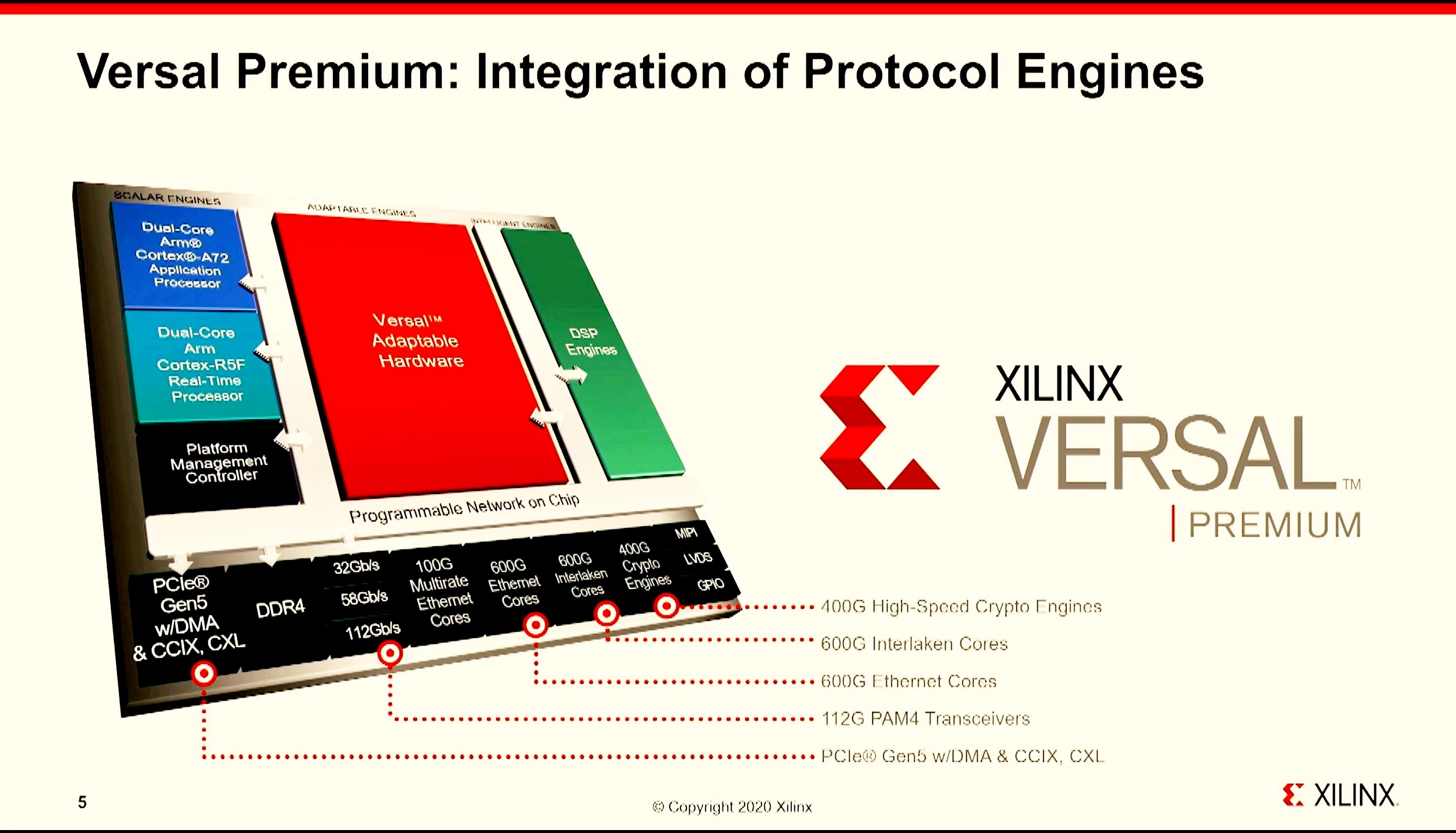
Xilinx’s traditional Versal device contains a number of scalar engines (Arm A72 cores for applications, Arm R5 core for real-time), intelligent engines (AI blocks, DSPs), adaptable engines (FPGA), and IO (PCIe, DDR, Ethernet, MIPI). For the biggest Versal products, these are large and powerful, facilitated by a programmable network on chip. For Versal’s AI Edge platform, there are two new features into the mix.

First is the use of Accelerator SRAM placed very close to the scalar engines. Rather than traditional caches, this is a dedicated configurable scratchpad with dense SRAM that the engines can access at low latency rather than traversing across the memory bus. Traditional caches use predictive algorithms to pull data from main memory, but if the programmer knows the workload, they can ensure that data needed at the most latency critical points can already be placed close to the processor before the predictors know what to do. This 4 MB block has a deterministic latency, enabling the real-time R5 to get involved as well, and offers 12.8 GB/s of bandwidth to the R5. It also has 35 GB/s bandwidth to the AI engines for data that needs to get processed in that direction.
The other update is in the AI Engines themselves. The original Xilinx Versal hardware enabled both types of machine learning: training and inference. These two workloads have different optimization points for compute and memory, and while it was important on the big chips to support both, these Edge processors will almost exclusively be used for inference. As a result, Xilinx has reconfigured the core, and is calling these new engines ‘AIE-ML’.
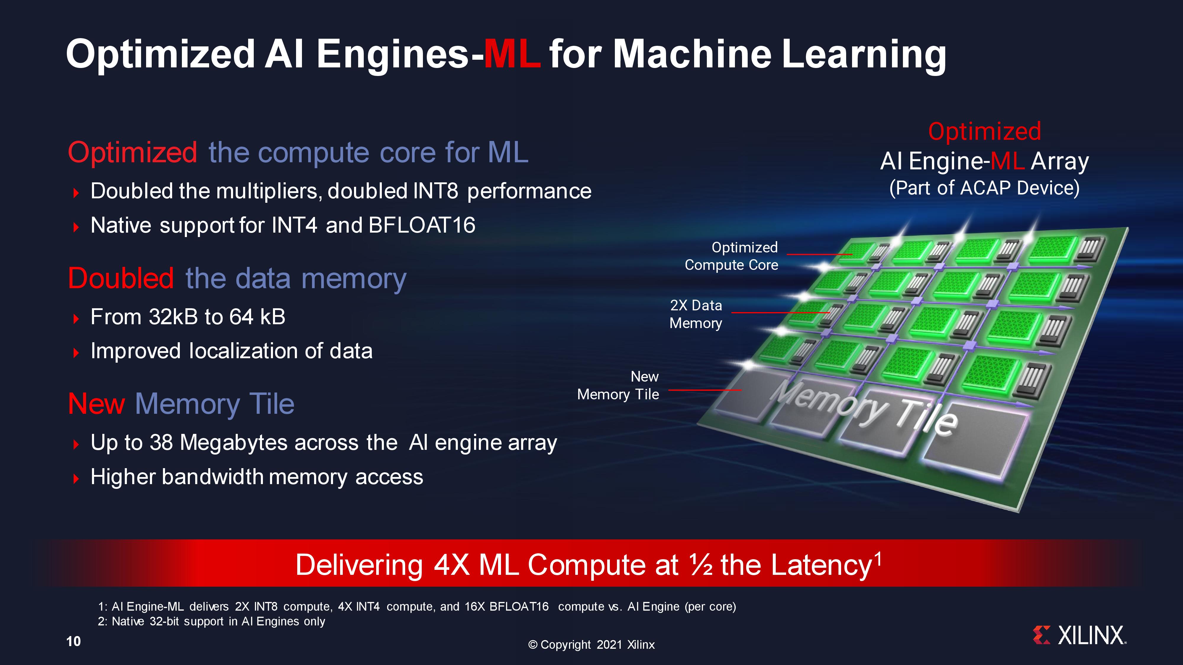
The simplest AIE-ML configuration, on the 6W processor, has 8 AIE-ML engines, while the largest has 304. What makes them different to the usual engines is by having double the local data cache per engine, additional memory tiles for global SRAM access, and native support for inference specific data types, such as INT4 and BF16. Beyond this, the multipliers are also doubled, enabling double INT8 performance.
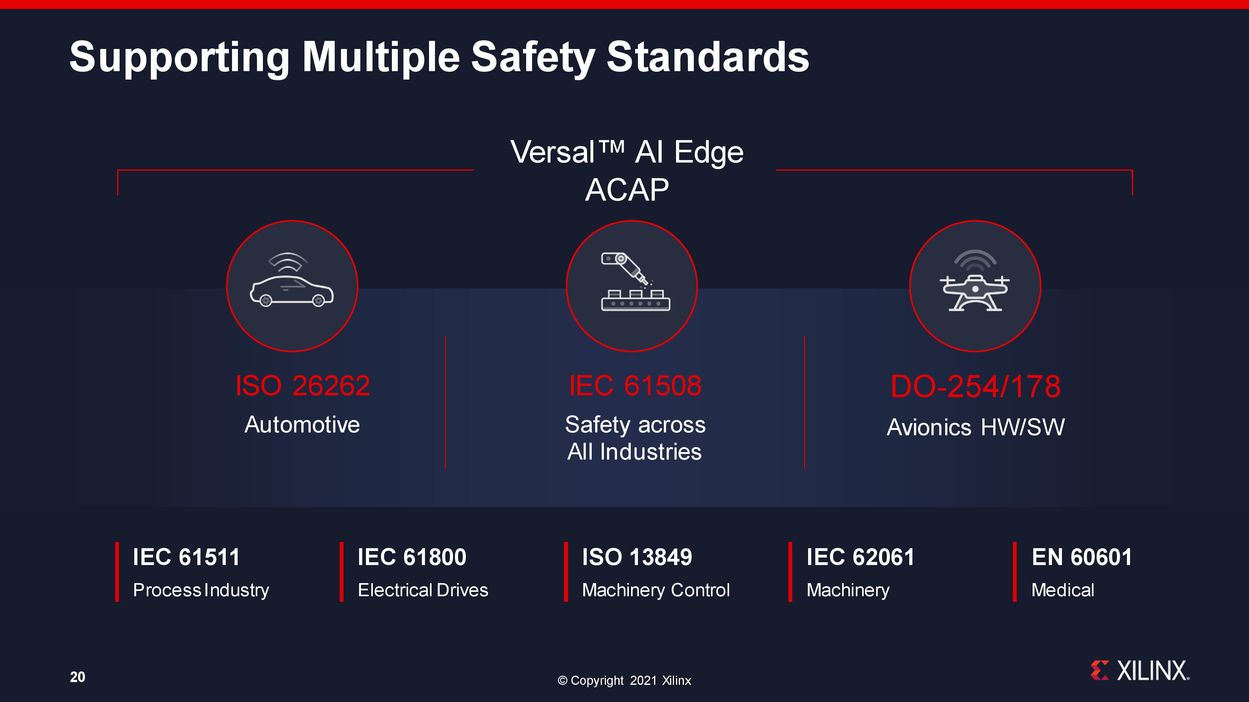
The combination of these two features means that Xilinx is claiming 4x performance per watt against traditional GPU solutions (vs AGX Xavier), 10x the compute density (vs Zynq Ultrascale), and more adaptability as AI workloads change. Coupled to this will be additional validation with support for multiple security standards in many of the industrial verticals.
Through our briefing with Xilinx, there was one particular comment that stood out to me in light of the current global demand for semiconductors. It all boils down to one slide, where Xilinx compared its own current automotive solutions for Level 3 driving to its new solution.
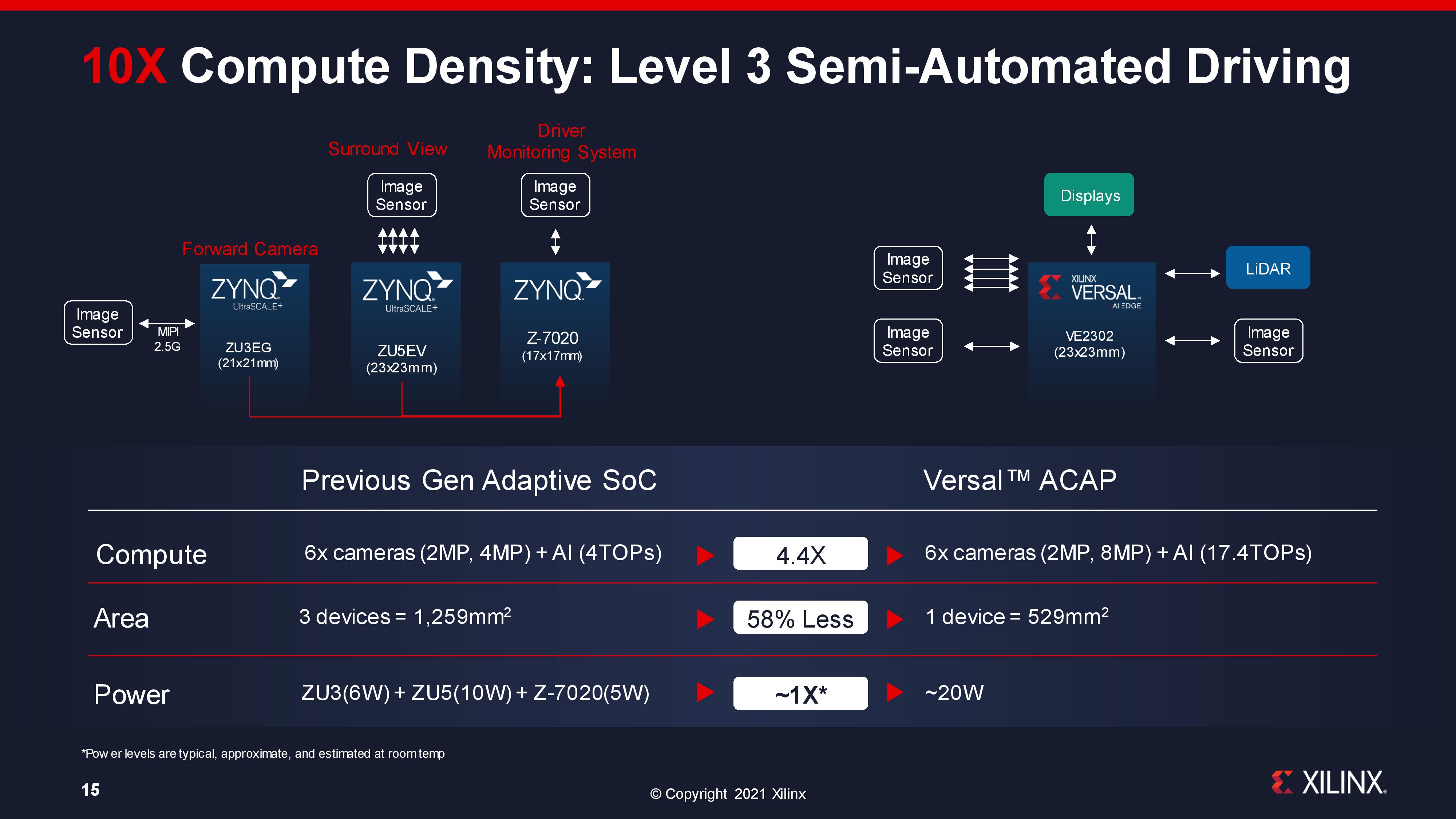
In this situation, to enable Level 3 driving, the current solution uses three processors, totalling 1259 mm2 of silicon, and then beyond that memory for each processor and such. The new Versal AI Edge solution replaces all three Zynq FPGAs, reducing 3 processors down to 1, going down to 529 mm2 of silicon for the same power, but also with 4x the compute capabilities. Even if an automobile manufacturer doubled up for redundancy, the new solution is still less die area than the previous one.
This is going to be a key feature of processor solutions as we go forward – how much silicon is needed to actually get a platform to work. Less silicon usually means less cost and less strain on the semiconductor supply chain, enabling more units to be processed in a fixed amount of time. The trade-off is that large silicon might not yield as well, or it might not be the optimal configuration of process nodes for power (and cost in that regard), however if the industry is eventually limited on silicon throughput and packaging, it is a consideration worth taking into account.
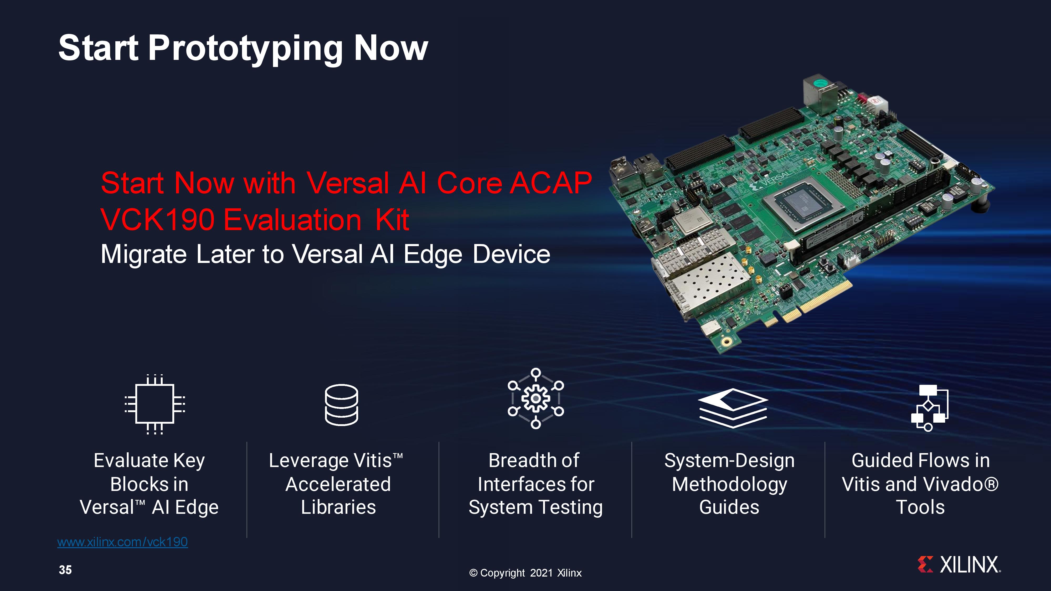
However, as is usual in the land of FPGAs (or ACAPs), announcements happen earlier and progress moves a little slower. Xilinx’s announcement today corresponds only to the fact that documentation is available today, with sample silicon available in the first half of 2022. A full testing and evaluation kit is coming in the second half of 2022. Xilinx is suggesting that customers interested in the AI Edge platform can start prototyping today with the Versal AI ACAP VCK190 Eval Kit, and migrate.
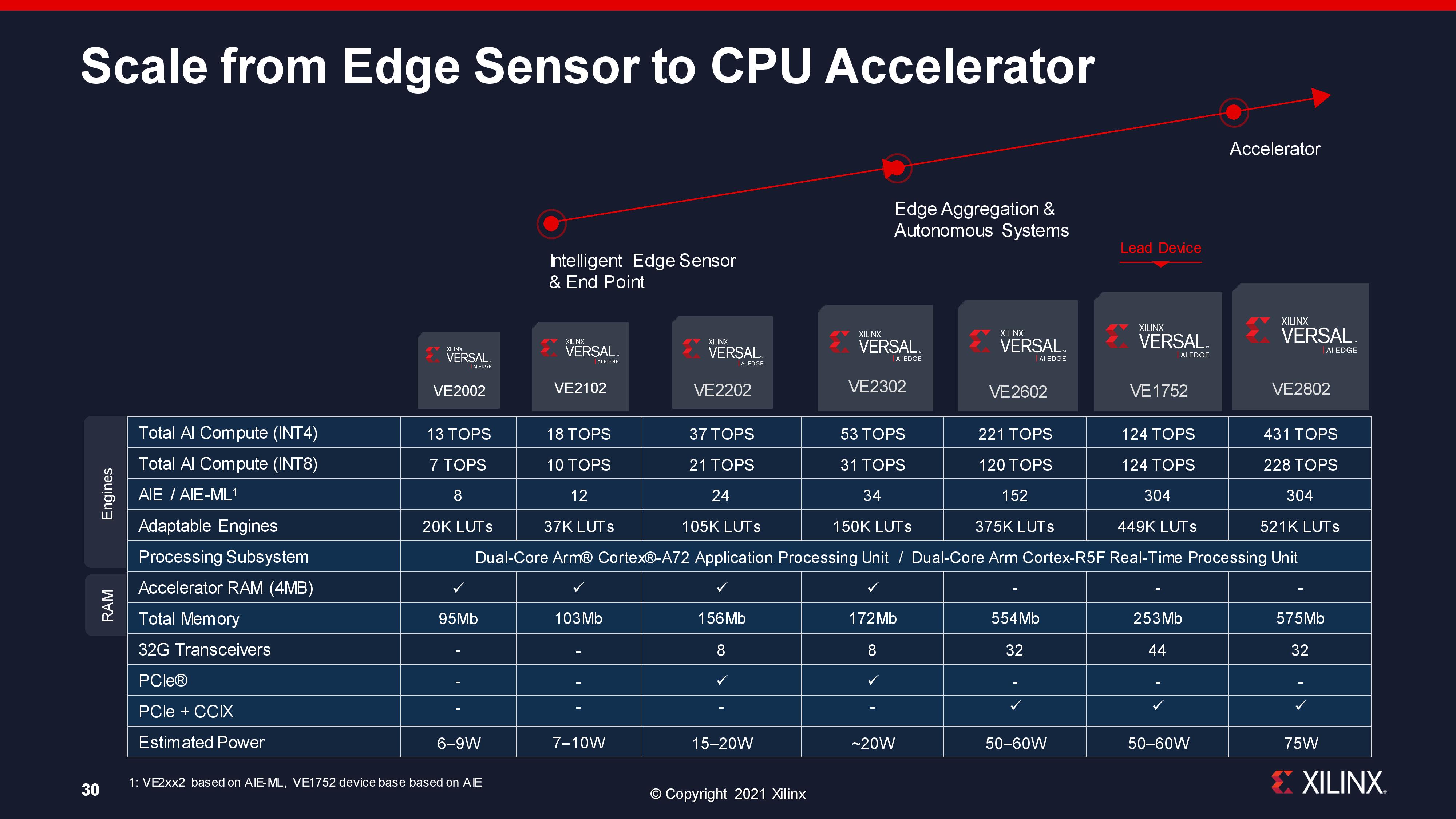
Full specifications of the AI Edge processors are in the slide below. The new accelerator SRAM is on the first four processors, while AIE-ML is on all 2000-series parts. Xilinx has indicated that all AI Edge processors will be built on TSMC's N7+ process.
Related Reading
- AMD in $35 Billion All-Stock Acquisition of Xilinx
- Xilinx Announces World Largest FPGA: Virtex Ultrascale+ VU19P with 9m Cells
- Hot Chips 31 Live Blogs: Xilinx Versal AI Engine
- Hot Chips 2018: Xilinx 7nm ACAP Live Blog
- Xilinx Acquires DEEPhi Tech ML Startup
- Xilinx Announces Project Everest: The 7nm FPGA SoC Hybrid
- NVIDIA Details DRIVE AGX Orin: A Herculean Arm Automotive SoC For 2022
- Marvell to Acquire Aquantia, Eying Automotive Networking Market
- Arm Announces Cortex-A65AE for Automotive: First SMT CPU Core


25 Comments
View All Comments
jeremyshaw - Wednesday, June 9, 2021 - link
> Helping solve the silicon shortagePaper launch, in the most literal sense.
GhostOfAnand - Thursday, June 10, 2021 - link
Worse still, they used ARM cores instead of going RISC-V.jospoortvliet - Saturday, June 12, 2021 - link
Old ones, A72... coming in 2022... pfft.BedfordTim - Wednesday, June 9, 2021 - link
Compare a future product with old ones and lo and behold it is better. I suspect Zync have a new and improved product as well.shabby - Wednesday, June 9, 2021 - link
"all built on TSMC’s 7nm processes"Stop wasting tsmc's capacity, you're not helping!
SarahKerrigan - Wednesday, June 9, 2021 - link
"Wasting"?shabby - Wednesday, June 9, 2021 - link
Yes wasting, their capacity would be better served making ps5's 😂shing3232 - Wednesday, June 9, 2021 - link
FPGA are use to design and testing new chips. What are you talking about?StevoLincolnite - Wednesday, June 9, 2021 - link
As a PS5 and Xbox Series X owner... Chips for the PS5/Series X is wasted capacity, we need more PC GPU's... Not Console chips that games can't take advantage of yet.Spunjji - Thursday, June 10, 2021 - link
I don't think anybody who cares about high-end desktop / mobile computing will mind them making these products on 7nm in 2022...