2023 Interposers: TSMC Hints at 3400mm2 + 12x HBM in one Package
by Andrei Frumusanu on August 25, 2020 4:00 PM EST- Posted in
- TSMC
- HBM
- CoWoS
- TSMC Tech Day 2020
High-performance computing chip designs have been pushing the ultra-high-end packaging technologies to their limits in the recent years. A solution to the need for extreme bandwidth requirements in the industry has been the shifts towards large designs integrated into silicon interposers, directly connected to high-bandwidth-memory (HBM) stacks.
TSMC has been evolving their CoWoS-S packaging technology over the years, enabling designers to create bigger and beefier designs with bigger logic dies, and more and more HBM stacks. One limitation for such complex designs has been the reticle limit of lithography tools.
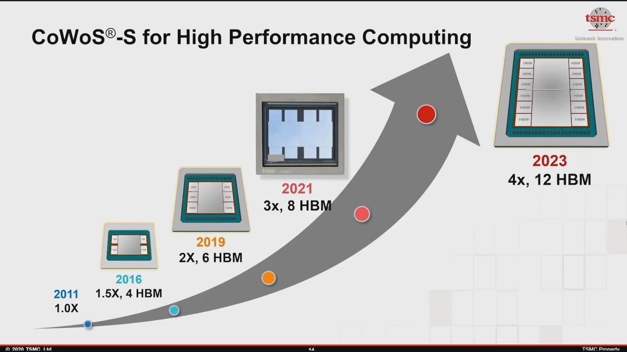
Recently, TSMC has been increasing their interpose size limitation, going from 1.5x to 2x to even projected 3x reticle sizes with up to 8 HBM stacks for 2021 products.
As part of TSMC’s 2020 Technology Symposium, the company has now teased further evolution of the technology, projecting 4x reticle size interposers in 2023, housing a total of up to 12 HBM stacks.
Although by 2023 we’re sure to have much faster HBM memory, a 12-stack implementation with the currently fastest HBM2E such Samsung's Flashbolt 3200MT/s or even SKHynix's newest 3600MT/s modules would represent at least 4.92TB/s to 5.5TB/s of memory bandwidth, which is multitudes faster than even the most complex designs today.
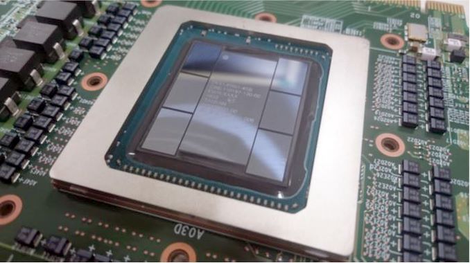
Carousel image credit: NEC SX-Aurora TSUBASA with 6 HBM2 Stacks
Related Reading
- TSMC Details 3nm Process Technology: Full Node Scaling for 2H22 Volume Production
- TSMC To Build 5nm Fab In Arizona, Set To Come Online In 2024
- TSMC & Broadcom Develop 1,700 mm2 CoWoS Interposer: 2X Larger Than Reticles
- TSMC Boosts CapEx by $1 Billion, Expects N5 Node to Be Major Success
- Early TSMC 5nm Test Chip Yields 80%, HVM Coming in H1 2020
- TSMC: 5nm on Track for Q2 2020 HVM, Will Ramp Faster Than 7nm
- TSMC: N7+ EUV Process Technology in High Volume, 6nm (N6) Coming Soon


34 Comments
View All Comments
melgross - Wednesday, August 26, 2020 - link
Um, no.FreckledTrout - Wednesday, August 26, 2020 - link
I have a feeling these designs will get the cost of HBM down. Eventually we will see similar designs for the client side as costs come down. I know it would be pretty awesome to have an APU with 64GB of HBM, a CPU and an GPU. TSMC's 3nm should make the power and densities possible.soresu - Wednesday, August 26, 2020 - link
Getting down the cost of HBM requires the process itself to be cheaper - it doesn't have anything to do with the capacity of any given process.For example, the latest Samsung V NAND flash generation dramatically reduced the number of process steps to make a wafer vs the previous gen.
This reduces costs, though we won't necessarily see that cost reduction as consumers.
What would make it cheaper is a V/3D multilayered DRAM device of some kind, which is something that is being looked into as DRAM area scaling becomes less viable - the problem is that HBM basically stacks multiple dies of DRAM on top of each other, which can't be nearly as economical as a layered monolithic 3D DRAM chip, any more than it would be for NAND flash.
With much denser single DRAM dies using multilayered 3D structures you could keep to only 2-4 high stacks rather than continually increasing stack height to keep pace with increasing demands for memory.
As it is 12 high stacks will be very expensive and few will use them.
Vitor - Wednesday, August 26, 2020 - link
If Apple combine this tech with their SoCs in 3 or even 2nm and we finally get solid state batteries, notebooks will get crazy good.