The Intel Lakefield Deep Dive: Everything To Know About the First x86 Hybrid CPU
by Dr. Ian Cutress on July 2, 2020 9:00 AM ESTA Stacked CPU: Intel’s Foveros
The previous designs of Intel, AMD and Qualcomm are what we call monolithic designs – everything on the processor happens on a single piece of physical silicon. When everything is on a single piece of silicon, it makes data management inside the processor a lot easier and simpler, it makes designing the processor a lot simpler, and manufacturing and assembly can be streamlined when only dealing with one physical element to the processor.
However, there have been moves in the industry to deviate from these single monolithic designs, as the benefits of trying something different are starting to offer beneficial points of differentiation within a product portfolio. It can lead to optimizations on different parts of the processor, it can be advantageous for cost reasons, and it also can expand silicon products beyond traditional manufacturing limits as well.
Monolithic vs Chiplets
You may be aware that recent AMD desktop processors are built on a ‘chiplet’ design. This is where multiple pieces of silicon are connected through wires in the green PCB in order to create a single ‘processor’. By using separate chiplets, each individual chiplet can either be focused on a single task (and be manufactured in the most efficient way for that task) or it can be a one of a repeated unit designed to scale out the compute performance.
For example, a processor core that contains logic circuits might aim for performance, and thus might require a very speed optimized layout. This has different manufacturing requirements compared to something like a USB controller, which is built to a series of specifications as per the USB standard.
Under a traditional monolithic regime, the single piece of silicon will use a singular manufacturing process that has to be able to cater for both situations – both the processor core logic and the USB controller. By having different parts of the overall design separated in different pieces of silicon, each one optimized for the best manufacturing scenario. This only works as long as the connectivity between the chips works, and it potentially enables a better mix of performance where you need it, and better efficiency (or cheaper cost) where you need it as well.
Of course, there are trade-offs: additional connectivity is required, and each chiplet needs to be able to connect to other chiplets – the total physical design area of the combined chiplets is often greater than what a single piece of silicon would offer because of these connectivity additions, and it could become costly to assemble depending on how many parts are involved (and if those parts are manufactured in different locations). Ultimately, if some chiplets are on an expensive manufacturing process, and some are on a cheaper manufacturing process, then we get the benefits of the expensive process (power, performance) without having to spend the money to build everything on that process, overall saving money.
One other benefit that a chiplet process can bring is total silicon size of the product. Standard monolithic silicon designs, due to the manufacturing process technologies we use today, have an upper bound of how big a single piece of silicon can be. By implementing chiplets, suddenly that upper limit isn’t much of a concern unless each chiplet reaches that limit - using multiple chiplets can give a total silicon area bigger than a single monolithic chip design. An example of this is AMD’s Rome CPUs, which total an area of over 1000 square millimetres, while the single largest monolithic silicon die is NVIDIA’s A100 GPU, coming in at 826 square millimetres.

NVIDIA's A100 GPU, with one big monolithic die and six high bandwidth memory dies.
Already in Market: AMD Chiplets
To put this into context of a modern design, AMD’s Ryzen processors use one or more ‘compute chiplets’ combined with a single ‘peripheral’ chiplet (often called an IO die). The compute chiplets are built on TSMC’s high-performance 7nm manufacturing node which extracts peak performance and power from the design. The ‘peripheral’ chiplet, which is not so peak performance focused but more tuned to standards like SATA, PCIe and USB, can be built on a manufacturing node where efficiency is more important, and also the cost can be lower, such as GlobalFoundries’ cheaper 14nm manufacturing node. Put together, these chiplets form a singular product.
AMD's Rome with 1 big IO die and eight compute dies
AMD had to overcome a lot of hurdles to get here, such as developing a chip-to-chip connectivity standard (known as Infinity Fabric), managing the power of the connectivity, but also physical manufacturing, such as ensuring all the individual chiplets match the same height for the heatspreader and cooler that goes on top to be effective.
One of the benefits of AMD going this route, according to the company, is that it allows them to scale the parts of their design that are easiest to scale for performance (the compute cores), and also manage where they think the future of compute is going. The other big benefit is that total die size of one of AMD’s server CPUs is larger than what can be manufactured in a single piece of silicon.
This sort of chiplet based approach also lends people to believe that AMD could swap out a compute based chiplet for a graphics based chiplet, or an AI-focused chiplet, and thus AMD could in the future offer different variants of its products depending on customer requirements for different workloads that the organization might have.
Coming to Market: Intel Chiplets
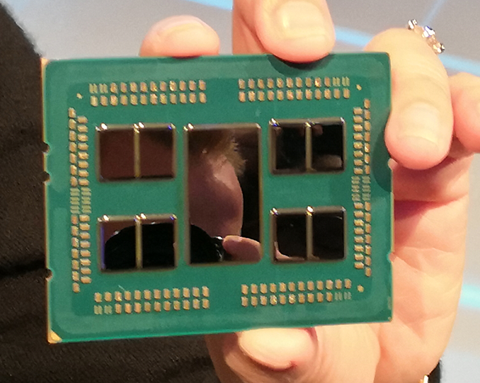
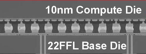
For Lakefield, Intel also goes down the chiplet route. But instead of placing the chiplets physically alongside each other like AMD, the chiplets are stacked on top one another. This creates a physically smaller processor package in the x-y dimensions, which is a critical component for laptop and small form factor mobile designs that Lakefield is aiming towards.
This stacked design replaces the tradeoff of physical space for one of cooling. By placing two high-powered bits of silicon on top of each other, managing thermals becomes more of an issue. Nonetheless, the physically smaller floorplan (along with a design focused to embed more control into the processor) in the x-y directions helps build thinner and lighter systems.
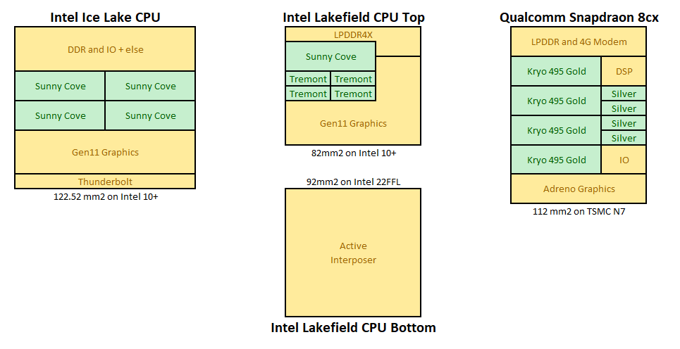
For the two stacked chiplets in the middle, the top chiplet is built on Intel’s high-performance 10nm+ manufacturing node and contains the 1+4 compute core configuration, as well as the graphics and the memory controller. The bottom chiplet contains the ‘peripheral’ components that are not as performance related, such as security controller, USB ports, and PCIe lanes. This is built on Intel’s cheaper 22nm manufacturing node.
Because this chiplet is on the bottom and has connections for power to pass through, Intel technically calls the lower chiplet an ‘active interposer’. An interposer is a term commonly used when chiplets are connected through a base piece of silicon, rather than through a green package PCB, because it allows communication between chiplets to be faster and more efficient, but it is a more expensive implementation.
What makes it an active interposer, rather than the passive interposers we have seen on some GPUs in recent years, is that it contains functional logic, such as the USB ports, the security, the chipset functions, and others. The passive interposers are just connection passthroughs, taking advantage of faster signaling. Active interposers include functional logic and have an associated power consumption that goes along with that.
The reason I bring this up is because there is some debate as to whether an active interposer is true 3D stacking as traditionally interpreted, or more akin to 2.5D stacking, which is what we commonly call a passive interposer. For those users who read more about Lakefield beyond AnandTech, you are likely to see both used.
Getting Stacked: DRAM and NAND vs Lakefield
The use of stacking is not necessarily new to the world of semiconductors. Both computer random access memory, such as DRAM, and storage components, such as NAND Flash, have implemented multiple layer technology for many years. What makes these elements different is the way they are stacked, plus also the power of the components involved.
The two main ways of stacking silicon together are through simple wire bonding, where the layers are not directly connected, or with Through Silicon Vias (TSVs), which are akin to stacks running through the layers.
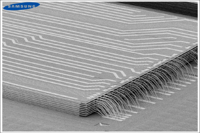
This is an image of Samsung’s NAND wire bonding technique, where multiple layers have separate connections to a base die. There is no direct connection between layers other than the act of physically coming together.

This is ‘Through Silicon Via’ (TSV) stacking, whereby each layer has a vertical channel that connects to the die above and below it. It allows for direct connection through the stack for fast access, which is useful when NAND has 64 or more layers. It can be quite difficult to do as well, but NAND manufacturers are experts in this methodology.
However, DRAM and NAND Flash are not the high-powered elements of a computer. Even the most dense memory configurations look to contribute single digit of milliwatts of power per layer when in use. Applying these techniques to high-powered computer chips is a bit more complex.
Stacking with Lakefield
What Intel is doing with Lakefield, with its stacking, is putting together multiple layers of high-performance compute into a single product. Also, while most DRAM and NAND Flash implementations stack silicon on top of each other, and then use external wire bonding or TSVs, to provide connectivity - for Intel’s Lakefield, the connectivity goes through the silicon, as with a traditional interposer (as mentioned above), and uses a die-to-die bonding to provide the communications.
Intel calls its stacking technology ‘Foveros’. It uses a novel design of die-to-die connectivity.
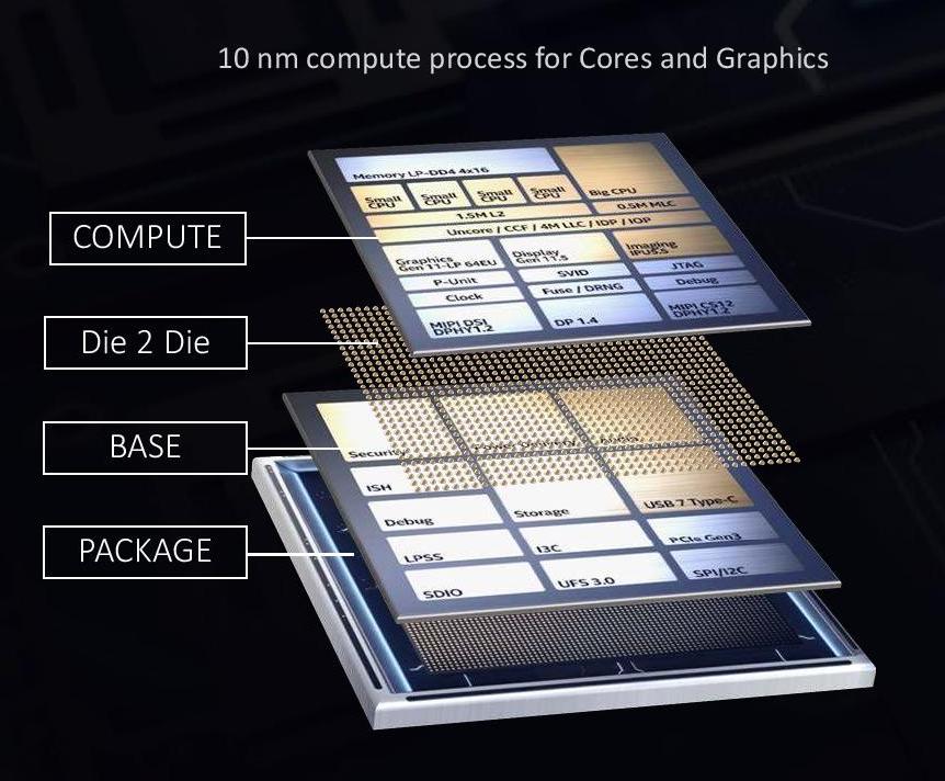
At the bottom is the base packaging material that connects all the signals going out into the system (power, USB, display). On top of this is the base silicon peripheral die, the active interposer, containing things like the USB control, storage control, security, and such.
Between the base silicon peripheral die and the top logic compute die is a method of connecting the two, in this case we have a solder ball array with a 50 micron pitch. This is essentially a ‘balls-on-balls’ technique, but with two silicon dies of different process node manufacturing techniques.
These connections will come in three flavors: structural, data, and power. Creating these bumps and ensuring they deliver what is intended is a hard problem – electrical issues, such as capacitance, and computational issues, such as maintaining a clock frequency, have to be managed, along with achieving targets in data rate bandwidth as well as power.

Here is the main introduction slide that Intel presented at the ISSCC conference regarding the die-to-die interface. Unfortunately these were the quality of the pictures as presented (the unreadable aspect ratios are also native to the presentation).
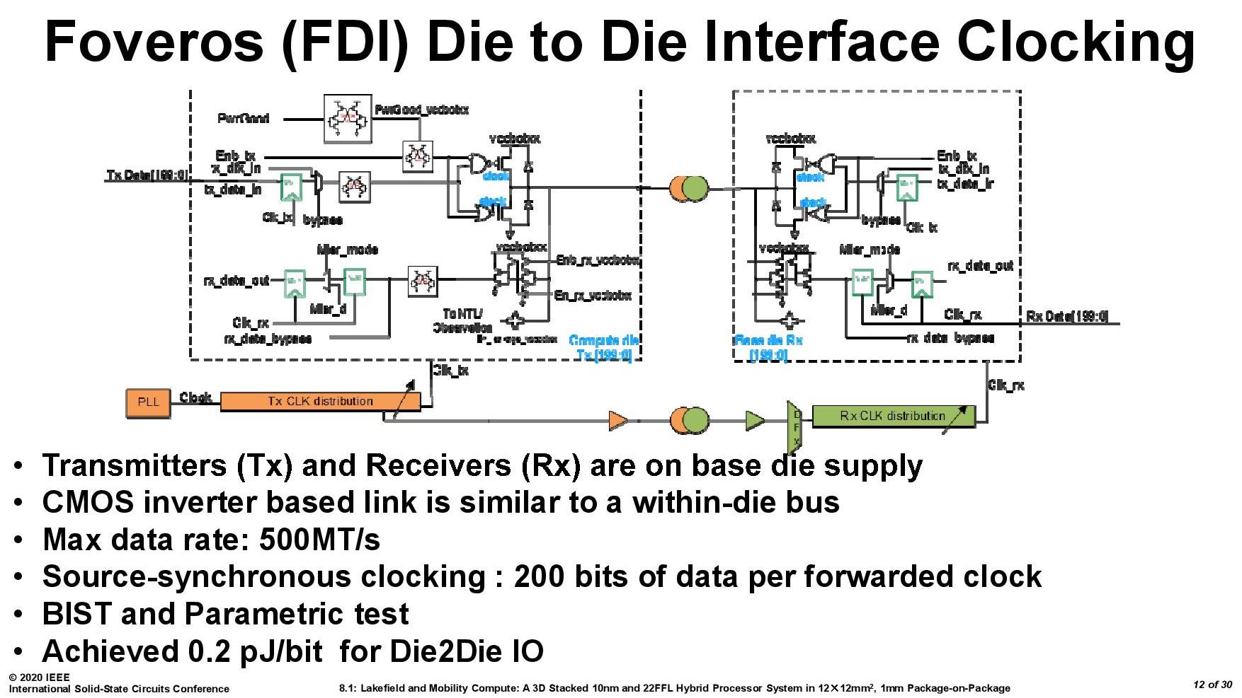
As mentioned, maintaining the clock coherency at speed and low power is a concern, and here’s what Intel did, with each connection operating at 500 mega-transfers per second. The key point on this slide is the power: 0.2 picojoules of energy consumed per bit transferred. If we extrapolate this out to a memory bandwidth of 34 GBps (maximum memory bandwidth of Lakefield), this equates to 54 millwatts of power for the data transfer.
0.2 pJ/bit is one of the benefits of keeping the transmission of the data ‘inside’ the silicon, but moving between the two layers. This is an order of magnitude better than the numbers quoted by AMD for its first generation EPYC server processors, which used data transfer links within the CPU package – AMD quoted 2 pJ/bit transfer by comparison.

Here’s a slide from Intel’s 2018 Hot Chips talk about new data transfer and connectivity suggestions. On the left is the ‘on-board’ power transfer through a PCB, which runs at 20 pJ/bit. In the middle is on-package data transfer, akin to what AMD did with 1st Gen EPYC’s numbers, around 1-5 pJ/bit (depends on the technique), and then we get on-silicon data movement, which is more 0.1 pJ/bit. Intel’s Foveros die-to-die interconnect is most like the latter.


221 Comments
View All Comments
AhsanX - Thursday, July 2, 2020 - link
The Sunny Cove has AVX-512 but Tremont cores don,t have any AVX. So Intel disabled AVX on the Sunny Cove core too, as heat was gonna be a problem if they let it enabled.ikjadoon - Thursday, July 2, 2020 - link
Did we read the same article? AVX-512 was completely removed (i.e., physically) from the Sunny Cove dies because of Windows 10 compatibility problems.Windows was never built for x86 heterogeneous processing and still cannot do anything close now in 2020 (perhaps that would've been a smarter investment than going all-in on touch in 2008!).
Intel & Microsoft remain stuck in late 2010s for their low-power / mobile-first / thin-client transition caused by the dominating success of smartphones & ARM-based architectures wiping out anything of interest in low-power x86.
There's a reason Intel just nearly stopped all development on Atom: nobody give a crap about the Pentium Silver & Celeron CPUs.
ikjadoon - Thursday, July 2, 2020 - link
*gaveJorgp2 - Thursday, July 2, 2020 - link
>There's a reason Intel just nearly stopped all development on Atom: nobody give a crap about the Pentium Silver & Celeron CPUs.Lol, no
ProDigit - Friday, July 3, 2020 - link
The $160 laptop I purchased from hp, with an N5000 in it, works really well!Would have been better if used on a desktop, and the core count was quadrupled.
extide - Thursday, July 2, 2020 - link
It's not a windows issue. Even if you ran Linux or any other OS on here you would have to run with CPU's all supporting the same ISA. ARM specifically designs cores to pair up together such that they have the exact same ISA (instruction support) so this isn't an issue in cell phones.I mean theoretically you could have the processors support a slightly different ISA and have it throw an interrupt if it tried to execute an instruction that the current core didn't support but a different one did and then the scheduler would have to move that thread to the other core. That could get really janky though, which is why nobody has talked about doing this yet.
Also, they said in this article that even though Intel said they removed the AVX512 units -- it can still be seen in the die shots.
Also, Intel didn't stop development on Atom -- this chip has a brand new core and their public roadmaps have several more in the future.
reggjoo1 - Tuesday, July 7, 2020 - link
They’re gonna have to develop more for atom, and get into the right “governor “ for crossover operation, more than scheduler tweaks. They have a lot to learn, and it may come down to the quality over the I/O system for these to really succeed. As long as their "ego" doesn't get in their way, and they learn from the "smartphone arena, they might have something for X86.dotjaz - Friday, July 3, 2020 - link
Did we read the same article? AVX-512 was clearly not removed.dotjaz - Friday, July 3, 2020 - link
There, "Intel has stated on the record repeatedly that they removed it. The die shot of the compute silicon shows that not to be the case." If you can read.jeremyshaw - Friday, July 3, 2020 - link
That was a later edit. Originally Ian claimed it was removed.