An Interview with AMD’s CTO Mark Papermaster: ‘There’s More Room At The Top’
by Dr. Ian Cutress on December 30, 2019 9:00 AM EST
On the back of a very busy 2019, AMD is gaining market share and is now a performance leader in a lot of CPU segments. The company has executed well not only with a good product but also at a time when its main competition is having manufacturing and production issues, which means AMD is ripe to push boundaries, gain market share, and make noise with a lot of wins. This year AMD’s Ryzen 3000 CPUs and EPYC Rome CPUs both have the new Zen 2 microarchitecture built on TSMC’s 7nm, something that might not have been possible without deep co-optimization between the two companies for a high performance product. AMD is also making strides with its relationships with enterprise OEMs. We touched on these topics (and more) with AMD’s CTO, Mark Papermaster.
 Dr. Ian Cutress AnandTech |
 Mark Papermaster AMD |
Mark and I have met several times over the last few years to discuss AMD’s strategy. His attitude is, perhaps correctly, a little reserved, but he isn’t shy of commending his teams design wins and is keen to talk up AMD’s partnerships and design strategies with corporate partners. In this interview, we cover product cadence, driving industry standards, partnerships between AMD and OEMs, and where the next of IPC could come from.
As always with our interviews, the transcription has been tidied up for readability and the questions may be rearranged to keep certain topics together.
AMD’s Release Schedule and Future Products
Dr. Ian Cutress: So far AMD’s rate of new products is on track to produce a new core almost every year. The roadmaps quite proudly showcase Zen 3 as almost ready, Zen 4 in development, and Zen 5 further out. Is this cadence sustainable?
Mark Papermaster: We’re on a 12-18 month cadence, and we believe that is sustainable. It’s what the industry demands from us.
IC: With the recent successes AMD has had, such as increasing market share in key areas and driving review, does that not perhaps give an opportunity to accelerate the cadence, hire more staff, or does it inevitably cause new ideas to form that slow down the rate of development?
MP: There’s a natural cadence to where we are, and we have multiple design/implementation teams in play. As one team completes, they move onto the next project. You know I think it’s the right rate for us, because in some markets you have an increased expectation of a new product every year, like smartphones. For that market you have to catch the holiday season every year with pretty much a new core, and to a large extent they can do that. But that need to tie things off at the same time every year means that there might be performance still left on the table for that core, and that’s going to happen every generation. So we believe we’re on the right track to deliver for our high performance customers, and that’s what we’ve based AMD’s resurgence on.
IC: Can you talk about how much of the roadmap has been penciled in for Zen 4 and post-Zen 4? Normally when we speak about these roadmaps, the 3-to-5-to-7 year roadmaps, the size of the company often determines the extent of the long-term vision, and over the last couple of years AMD has been quite active in promoting its three-year time span.
MP: What we share publicly, the current roadmap, shows our trajectory and what we’re doing for the current generation, but also n+1 and n+2. You know, of course we have teams that are looking beyond n+2, but we don’t really talk publicly about what we’re looking at that far out. The biggest change for AMD compared to how we used to do things years back is that we have a constantly leapfrogging set of design teams, and this helps us to have this constant innovation process to say on the 12-to-18 month cycle, taking the time to make sure that we have the right performance for the hardware that we’ve come up with. If we get to a point where we have to square off a design due to time-to-market, then the ideas that don’t fit in that window get rolled right into the next generation team.
IC: Recently an interview with an AMD executive related the current roadmap as a sort of tick-tock model, based on what Intel used to run for a decade. Do you have parity with this analysis?
MP: I didn’t see the particular interview you’re referring to, but what I will say is that we’re not on a tick-tock model. What we’re doing is looking at each generation of CPU and marrying the best process variant that’s out there with the right set of IPC improvements, memory hierarchy, and all the things that we can put in there. We are committed to staying on the best possible pace of improvements each generation that we can. This is a formula that’s working well for us at AMD.
IC: Should we expect Zen 2 to have a refresh, like a Zen 2+, like Zen 1 did?
MP: I have nothing to say on any refresh on current designs, but we always look at where it makes sense and where we’re able to take opportunities to provide a bump in performance, power, or die area.
Driving IPC and Performance
IC: During a recent earnings call, Lisa mentioned that moving forward AMD won’t always be relying on taking the best process node advantage from TSMC, and the company will be driving architectural improvements as time goes on. In order to drive leadership through these last two generations and into Zen 2 and beyond, you’ve been driving microarchitectural IPC aggressively – is that in of itself sustainable, as we move into an era of diminishing return for increased core counts?
MP: So clearly the industry has figured out how to take advantage of increasing cores. There is a rate and pace that as a CPU vendor you have to manage with this because you cannot increase the rate of change of the number of cores at a faster rate than the software can take advantage of it! But we’re clearly adding more engines on CPUs and GPUs, and those specific hardware engines will remain a force going forward. Now it clearly has to be done in a balance with memory and IO – we have to be able to provide a balanced system. We know this very well at AMD, and that’s what we’re going to keep doing.
IC: One of the things that drives new generations of hardware for everyone, especially processor architecture, is improvements to the ISA and new instructions. But as we’re also seeing specific accelerators being bundled on packages, and additional security hardware and such, how is AMD going to drive that arm of the industry forward?
MP: If you look at our chips today, we have a variety of specialized functions. Every AMD chip has a PSP, a platform security processor, which as you know is an isolated processor within our silicon for root of trust and providing security services. We also have accelerators in our cores designed for specific math functions. We also have a number of DSPs that we focus on that our notebook chips have and will have, and our client processors will have audio processors on there. So it’s a matter of ‘when does it make sense’ to have an accelerator or a specialized function on the silicon, or perhaps even as a chiplet? We’ve led the way in the chiplet architecture for various segments, so we understand when it makes sense to have something discrete and/or keep it under evaluation until it needs to come on-module or on-chip.
IC: AMD is very proud to have an IPC advantage on the desktop today with Zen 2, but we continue to see Intel pushing the boundaries of new ISA instructions, such as vector instructions or bfloat16, because Intel has to cater for those edge cases and customers that really want the specific features. AMD has had much success in the past, such as driving the 64-bit x86 standards. Can we see AMD being a force behind defining future x86 instruction standards?
MP: We continue to look at every facet of design. If you see the security innovations that we brought out with the Zen processor line, with memory encryption – we drove capability that did not require new extensions as it was under the covers and didn’t need to drive a set of software modifications. So we look at innovations that can benefit the end customer, and some of them do in fact need an extension so we continue to look at that. On the overall viewpoint for x86, we’re always looking at some extensions that drive wide adoption, and if that happens, we include it.
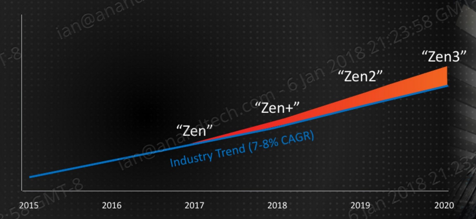
IC: Everyone’s favorite topic when discussing new hardware is about increases in IPC. For Zen 2, we saw a very good 15% increase in IPC over the previous generation. Recently we heard about Forrest Norrod (SVP of Datacenter) talk about Zen 3, in that we should expect to see a very typical increase in IPC again, making another step-function improvement over Zen 2. Do you expect AMD to continue with these sorts of improvements?
MP: So with our roadmap, and as you know I won’t go into specifics about IPC gains for future generations, but we are driving a model of high-performance compute, and there will be performance gains with each new generation. It’s all about picking the right set of IPC improvements, and the right process nodes and design rules for our core designs. There’s always a balance when we design our cores, so match power with efficiency, and at AMD we still expect to exceed the industry standard. We’ve stated before that the industry has been on a slow 7% annual growth rate in single threaded performance, and our goal is to beat that with every generation of our products. We’ve executed better than the industry with our recent products and we exceeded industry expectations.
(It’s worth noting that at a 7% annual improvement needs to be met, if a new product comes out every 18 months, then to stay on the same trend each product needs a +10.7% improvement.)
IC: As core performance increases, it puts extra stress on the caches inside the core. AMD has done well with respect to cache size and latency, such as the large L2 in the current designs. We now have a situation where your main competitor has increased its L1 cache size by 50%, in exchange for a 25% increase in latency right at the heart of the core, which was a big surprise to us. Can you talk about AMD’s cache design momentum, and your thoughts on this?
MP: As your saw, our Zen design from first gen to second gen has improved our memory hierarchy and associated latencies. We have that focus, and I’m not going to pre-announce what’s in Zen 3, but the cache design is a part of that overall IPC uplift that we talk about, and part of the performance improvement that we focus on every generation. Latency matters for our customers, for sure.
IC: One of the key marketing messages that AMD has had since Kaveri is to hit its 25x20 goal: to enable 25x more performance on its 2016 products by the end of 2020. We’ve been following this goal closely, and it still seems as if AMD has a way to go. Can you comment on this?
MP: I’m actually really excited with how our team has rallied around this message. Our engineers actually called that goal, it wasn’t initially a marketing message at all. They’ve used it as a motivating factor in driving the notebook advantages of all the design and the process aspects that go into every generation. So yes, we’re excited about the progress we’ve made, and if you look at our second generation of Ryzen Mobile that came out, I think what you saw was excellent with improvements in battery life and performance. Then you have to look at the deep partnership with Microsoft on the Surface Laptop 3, and that enabled yet an even closer software and hardware partnership that benefits not only Microsoft but also the Windows ecosystem. That partnership has resulted in an even closer power management interlock across all of AMD’s mobile offerings with Windows.

On-Package High Bandwidth Memory and Semi-Custom Designs
IC: Are we at a point in time where processors need on-package high-bandwidth memory? We’re seeing memory channel counts going up and memory frequencies going up, and we’ve transitioned from DDR3 to DDR4 and moving into DDR5 in the future, but there’s still a segment of the market that wants high-bandwidth memory as close to the processor as possible.
MP: You bet, and we’ve been in this space for years. We led the way at AMD of bringing HBM to GPUs – it’s on a silicon interposer using a 2.5D packaging technique. What makes it critical is getting the right memory solution for the workload, and you also have to hit the right cost/performance targets. It’s a tricky balance that you have to make for every product. In high performance GPU computation, HBM is a must, and you see it on our MI roadmap. At every other point, we always look at the right solution, and both GDDR and DDR have great roadmaps that are being executed on, and we’ve been leveraging these technologies successfully. We will do the same moving forward, looking at each of our products and asking where the industry is going, what the workload requirements for each product are meant to be, and what are the cost/performance metrics of each memory solution.
IC: We’ve seen some customers go down the AMD route already implement GDDR with your CPUs and APUs, such as with the Subor console and other console-like chips. If a HPC customer came along and wanted HBM on the CPU package, would that be something you would consider?
MP: For our semi-custom business like that, when a customer has a volume opportunity and wants to partner deeply to leverage the building blocks that we have, then if it’s a great opportunity for both companies involved we will create a semi-custom solution. We continue to analyze those opportunities as they come up.
IC: What level of investment is required for a partner to invest in a semi-custom chip? I know that’s a super broad question, but we’re trying to understand what a company like Zhongshan Subor (now defunct) had to invest to be able to get a semi-custom design. Is it millions, or 10s of millions? Surely someone with 50 grand isn’t going to be in semi-custom.
MP: I’m unfortunately not able to answer that. These types of agreements we have in place are confidential. But you are correct, it’s more than 50k! As you know, if you want to be on the leading edge with these designs, just creating the masks can cost millions.
IC: From our perspective, it’s hard to discern with these agreements how much the partner is putting in compared to what AMD is putting in: does the partner get a good deal if it’s a unique design and AMD sees interest in that design outside of the partnership, or are all the costs borne by the partner? The Zhongshan product was reported (albeit unverified), to be in the 30m range, which meant that if they funded all of that, they would have to sell a good million or two million units to break even, which didn’t seem feasible.
MP: I can’t say much, but I hear what you are saying. Our semi-custom agreements, even if we’re collaborating just on hardware or it’s the full stack, ultimately remain confidential and it’s up to the customer about how much they want to say. All I can say is that our semi-custom model is alive, successful, and a key part of AMD’s offerings.
Compute eXpress Link (CXL)
IC: AMD is now a member of the CXL consortium, even though it’s also a member of pretty much every interconnect standard in the market, and in the past AMD has pushed CCIX. CXL has strong ties to PCIe 5.0, so can you talk about AMD’s expectations and deployments of these new interconnects?
MP: AMD is a proponent of open standards that align with the industry, especially when it comes to common standards for IO and accelerators. You’re absolutely right in that we joined CCIX and we have been active there – but we’ve been active in almost all the consortia we are a part of. On CXL, we joined and we believe it’s actually a very strong consortium to leverage PCIe 5.0. We are also very strong participants in PCIe development efforts, so this aligns with our strategy of leveraging PCIe by also being able to craft, through a consortium, a lower latency interconnect standard that is the best way for the industry to drive alignment and leverage that PCIe foundation. This is what is going to drive the PHY (physical layer) development – it can be a huge cost but being part of both of these standards helps us amortize those PHY costs, as a path to both low-latency accelerators and memory compared to standard PCIe. So we think it’s a good consortium, and I do see it gaining momentum in the industry.
IC: Do you expect CXL to align with PCIe extensively over its lifetime?
MP: We’ll see – watch this space. When you look historically, often these types of consortia start off from one of the larger standards committees, they have in the past emerged into a broader standards committee in of themselves, but it’s way too early to make that call for CXL.
IC: One concern over the diagrams shown for CXL is that in the future, there might be CXL-only accelerators, like CXL-only graphics cards and CPUs, that won’t support PCIe 5.0. What’s your opinion of this?
MP: It’s good to know that concern – I don’t see that happening. Any device that is CXL compliant will also be PCIe compliant (and actually requires a PCIe handshake to initiate the protocol), so any additional limitation would be vendor specific. But we don’t see that happening.
Frequencies and Moore’s Law
IC: One of the concerns raised when moving to more advanced process nodes with similarly designed cores is a loss in frequency due to current density. When AMD moved to TSMC’s 7nm the company made some noise about how it was able to keep frequency parity with the 14nm/12nm designs from Global Foundries. Compared to previous generations of Ryzen, you’ve even pushed those frequencies higher. Elsewhere in the industry we’re seeing difficulty in keeping frequency parity on the newest process nodes – so even though PPA (power, performance, area) improves as a whole, how does AMD approach that issue for future process nodes? Are there any additional factors that we should know as the public and as engineers that follow this space that AMD has taken into account?
MP: I think that when you look at all the commentary about Moore’s Law, you see pretty much universal alignment that we no longer have the old Moore’s Law we’d all come to know and love, the one with a frequency improvement in every generation and the advantages of power and area that came along with those frequency improvements. In this new era, it’s not that Moore’s Law is dead as such, but it’s not the same old Moore’s Law. There is somewhat universal alignment now that frequency is already not scaling with each successive node – I think that most in our industry accept that as a given.
What that means at AMD is that we design our plans such that we can take a holistic view at all the levers we have to drive performance up. This is why we’ve innovated on chiplet approaches – we apply that to where it makes sense. That’s why we’re innovating on changes that we make to our memory hierarchy, and as I’ve already mentioned, carefully choosing the right type of memory we deploy for specific workloads. It’s this type of holistic system approach that we’ve adopted and going to add to as we move forward to make sure that even in this new era of Moore’s Law that we operate in, we can continue our drive to higher performance.
New Generations of Infinity Fabric
IC: AMD’s Infinity Fabric (IF) is a key part of the messaging when it comes to AMD driving scalability between its products and AMD fellows do delight in talking about it. As we move to new faster connectivity standards, like PCIe 5.0 and even PCIe 6.0, will IF keep pace with driving bandwidth, or are we going to be blowing through the power budget just on interconnect?
MP: What you flag is certainly a concern across not only the Infinity Fabric (which is AMD’s protocol and a key in our chiplet approach) but also flexibility and modularity that we have across our roadmap to get our latest generations of our intellectual property into all the segments we serve. So there is a reason why we increment and design a new version of IF for each generation of product – it is in fact the innovation required to keep growing the bandwidth and yet keeping the overall system optimized. You also have to do the same with the IO and interconnects that you drive off chip, like the PCIe and all these SERDES links. They require that same innovation. I think you’re seeing a lot of work on our design approach on both logic as well as our SERDES, for both long reach and short reach implementations.
IC: With every new generation of Zen, would it be safe to assume that we should expect new generations of Infinity Fabric to partner them?
MP: That would be my expectation.
IC: In the market today we have dual socket Rome using IF for socket-to-socket communications, and we’ve been told that the GPU line will enable GPU-to-GPU infinity fabric links at some point. Is there a technical reason we don’t see CPU-to-GPU infinity fabric connectivity right now?
MP: So we deploy IF in both CPU and GPU, and it enables us to scale very effectively. We leverage across CPU and GPU today, and it allows us to use elements of optimization that we can do using the protocol. We continue to look at where we can leverage that benefit, and where having an AMD CPU connected via IF to an AMD GPU makes sense.
Manufacturing Partnerships
IC: Is AMD a key partner for TSMC’s 5nm production?
MP: We haven’t announced a 5nm part at this point, but we work very closely with TSMC, and you’ve seen the kind of deep partnership that we have with them with 7nm across our product lines.
IC: It has been announced that AMD is partnering with Samsung regarding mobile graphics. Is that purely a hardware relationship, or does it extend to manufacturing?
MP: The partnership with Samsung is an IP joint venture. We’re partnering with them on that with our graphics IP. As you know, AMD is not in the smartphone business, so that joint venture will result in technology that is then deployed by Samsung into their products.
IC: From our audience, one of the most common questions I need to put to you is about TSMC’s capacity. Can you shed some light into how this might affect AMD?
MP: TSMC is a key partner for us, and they were with us at our second generation EPYC launch. I think that really helped people to understand the scale that TSMC has. The most rapid launch in the history of TSMC was its 7nm process node, which has had an asymptotic volume ramp and that was well ahead of our launch of Rome and EPYC. So we’re getting a great partnership with TSMC, as well as great supply. We did have some shortfalls on chips when we first launched our highest performing Ryzens, and that was simply demand outstripping what we had expected and what we had planned for. That wasn’t a TSMC issue at all.
IC: We’ve seen reports of TSMC extending lead times for order requests? Does that put a spanner in the works for 2020/2021 launches?
MP: Part of our close relationship with TSMC allows us some insight into what they’re able to offer and when; but we also have to leverage our planning team and they have to be on the ball with every product and every launch. Just so you know, that’s always going to be the way: lead times for not only popular nodes but also the leading edge nodes go up every generation. As a result, everyone, not only at AMD, has to get better and better at this.
AMD’s Market Share
IC: A number of media and analysts have been looking at AMD’s rise in both product performance but also strategy when it comes to the enterprise. They’ve been waiting for AMD to catch up and provide healthy competition, which it is now doing, and now we’re looking at when your competition will catch up to you. Despite this, we still see AMD’s enterprise market share growing perhaps slower than expected. Is there a reason for that? Or are we still in a miasma of teaching people that AMD is back in business, or a victim of slow enterprise update cycles? Can you shed some light?
MP: If you look at the server market, we said that we projected in about mid 2020 that we would hit double digit market share. People have asked us why does it take that long, and why we aren’t moving more quickly, and the fact is that it takes longer in the data center markets to bring the partners along and get through their entire certification cycle to get their customer work cases and applications optimized. We’re actually really incredibly pleased with the response from the OEMs and customers, and with our second generation EPYC, with Rome, we’re right on track with our expectations, and the market is growing too.
What’s the Limit?
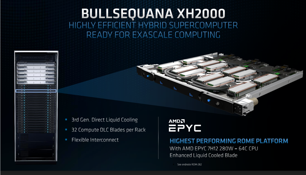
IC: AMD’s current highest TDP processor on the market today is at 280W, such as the EPYC 7H12 built for HPC. Is there an upper limit to TDP expansion? We see Intel moving into the market with higher TDP chips, at 350-400W TDPs.
MP: Collaboration with our OEM partners isn’t just about maximizing the power available for the CPU. You also work across both CPU and GPU, and that’s what we’re doing with Cray/HPE for the Frontier supercomputer. That’s really indicative of the kind of system optimization across hardware and the system and software stacks that we can do with OEM partners to really push up the roof in the HPC market.
We announced that 7H12 part in our continued roll out of Rome, and you saw ATOS use it and we were really happy for them to see their placement to catch the Top500 listing as it was a race against time, but it just shows what you can do with great execution. But you know when you think about that time of integrated water cooled solution, it tells you that you have to grow these close partnerships, as we’re doing at AMD with our OEM customers, and there’s a lot more performance that can be had going forward. There’s a lot more room at the top!
Many thanks to Mark and his team for their time.


68 Comments
View All Comments
Kishoreshack - Monday, December 30, 2019 - link
Why are the release schedule of Zen 2 desktop parts& Zen 2 Mobile parts Sooo distant from each other
why doesn't AMD releases them together
or at least at one month apart
Ian Cutress - Monday, December 30, 2019 - link
They are two completely different designs on silicon. You can't just magic them up overnight.deksman2 - Monday, December 30, 2019 - link
Actually, mobile designs aren't that different vs their desktop counterparts.They do have an iGP which changes things around, but the overall CPU part is still the same.
And also, if Zen 2 design was completed long before its release, then AMD would also have a mobile lineup designed at the same time.
All it comes down to really is production at this point.
But its possible that supply issues with 7nm have caused delays... plus there was a chemical spill early on which contaminated large amount of wafer batches, and huge orders from other companies such as Apple.
Its possible things might change a bit with Zen 3 which uses 7nm+... and most notably after that Zen 4.
Ian Cutress - Monday, December 30, 2019 - link
I'm glad you're telling me the mobile designs aren't that different. I wouldn't have known otherwise! I mean, I only cover AMD's product line in-depth. /sOne of the big issues is going to be around power on the chip, because managing power between CPU and GPU on the same die is a drastically more complicated issue than just CPU alone - there are various ways to do with with in-die LDOs, on-die regulators, on-package regulators, and therein all the sensor requirements to deal with current density hotspots generated from the design that have different ramp up functions from just a CPU-alone model. Then there's the fact you have to have masks created for the design, which in of itself is a big cost. But then we should also talk about any shared cache design, or the security aspects of the PSP dealing with different cores and different stages of memory access...
I could go on
and on
and on
It's not as simple as you make out. There is a reason that hundreds if not thousands of people work on every little detail, because an error in silicon isn't always solvable.
twotwotwo - Monday, December 30, 2019 - link
FWIW, Andrei of AT mentioned on Twitter that his Ryzen chip appeared to have about 17W power draw at idle: https://twitter.com/andreif7/status/11554204423599... -- this sort of lines up with things AT has previously mentioned about uncore/interconnect eating nontrivial power under even light load. (Ian kind of alludes to it in some questions about IF.)Not a huge deal in a high-performance desktop, but a dealbreaker in mobile. And so another thing for the list of changes to put a core into a mobile chip.
ksec - Monday, December 30, 2019 - link
1. The Mobile Variant is a Single Pieces of Silicon with GPU and Memory Controller, so it is entirely different to the Desktop and Server.2. The Mobile Variant is also on a different node, even though they are the same 7nm, one is HP another is LP. Where LP stands for low power.
3. Lower Margin on most Laptop CPU, ( comparatively speaking ), AMD is basically making one Die, for Desktop and Server Market, both are higher margin market and just so happens AMD does them with lower cost and giving them another competitive advantage.
4. High Margin Laptop CPU is basically dominated by one vendor, Apple. AMD is not in the Apple ecosystem yet.
5. AMD is small and has limited resources. So I dont blame them for taking the path which leads to more profits first.
Zibi - Monday, December 30, 2019 - link
Mobile is different - not only CPU alone has fewer cores and smaller power envelope but you also need to include the cost of the whole platform. You need chipset with less power demand than X570, you need to include NIC, WiFi, etc. Intel had Centrino and now it has Athena - AMD has nothing like that. It means that for mobile AMD needs to transform their solution - maybe make it more SOC-like like in the server space. Servers with AMD CPUs do not have chipset -> everything is driven from IO Die. Server CPUs though have bigger prices and as everyone here agrees in mobile space margins are thin (and Intel really can dough money to OEMs to not to be too creative with AMD). I really would like to see AMD changing the mobile market the way they changed servers and desktops. It's not that easy though and it's better people realise that.BTW @Ian is it possible for you to ask whether the IPC uplift for the next gen will be the same for server and for desktop CPUs ? I see some obvious possibilities to increase the performance but they are more one the server side.
AshlayW - Tuesday, December 31, 2019 - link
We've got an armchair Silicon engineer here.Kishoreshack - Monday, December 30, 2019 - link
Shouldn't AMD also work on their own FAB ?Too much dependency on TSMC is causing it trouble?
Ian Cutress - Monday, December 30, 2019 - link
AMD used to have its own fabs. Due to financial issues they were spun out and are now called Global Foundries.