Intel Q3 2019 Fab Update: 10nm Product Era Has Begun, 7nm On Track
by Anton Shilov on October 28, 2019 9:30 AM EST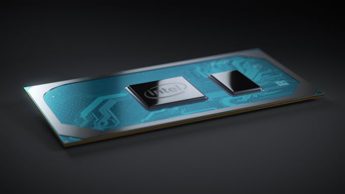
After years of delays, Intel is finally shipping its 10 nm processors in high volume, and the company is preparing to fire up another fab to produce an even larger volume of 10nm products. Along with producing more of the company's existing Ice Lake-U/Y products, Intel is also planning for server CPUs and GPUs as well, with Ice Lake-SP CPU as well as the DG1 GPU already up and running in Intel’s labs. Meanwhile, even farther out, Intel is eyeing 2021 for the rollout of its EUV-based 7nm process.
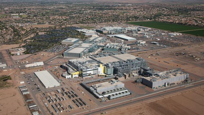
During its earnings call on Thursday, Intel said that so far 18 premium systems based on its 10th Generation Core (Ice Lake) processors have been formally introduced and 12 more are expected in 2019. Right now, the company produces all of its 10 nm CPUs in Hillsboro, Oregon and Kiryat Gat, Israel. Starting next quarter, the company expects 10 nm chips to also ship from its Chandler, Arizona, fab, which will increase supply of Ice Lake processors and will get Intel prepared for a broader use of the manufacturing process that had caused company a lot of troubles.
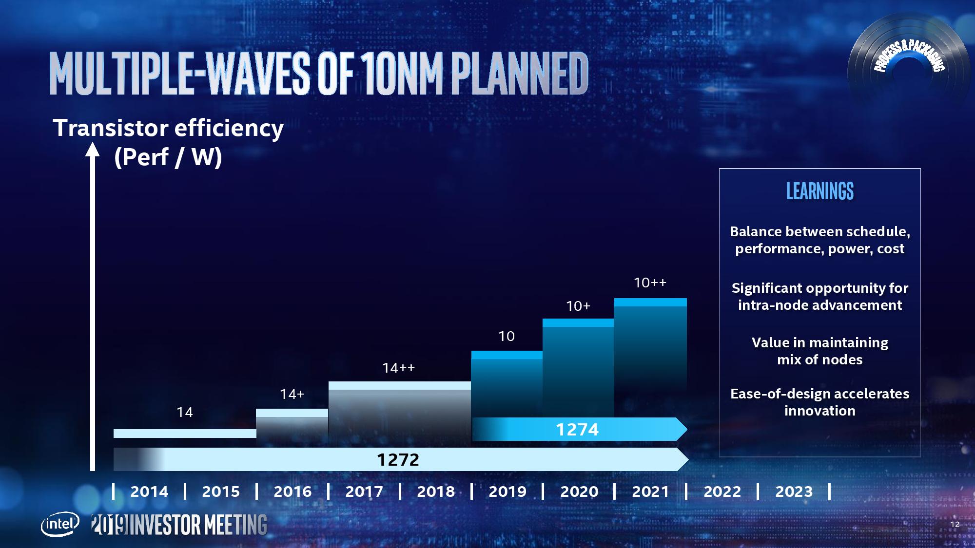
In addition to client Ice Lake CPUs and Agilex FPGAs that are currently shipping, Intel’s 10 nm portfolio includes datacenter-grade Xeon (Ice Lake-SP) processors due in the second half of 2020, discrete DG1 GPU(s), an AI inference accelerator, and a 5G base station SoC. One thing to keep in mind here is that Intel will use different iterations of its 10 nm technology to make different chips.
Here is what Bob Swan, CEO of Intel, said:
“The Intel 10 nm product era has begun and our new 10th Gen Core Ice Lake processors are leading the way. In Q3, we also shipped our first 10 nm Agilex FPGAs. In 2020, we will continue to expand our 10 nm portfolio with exciting new products including an AI inference accelerator, 5G base station SoC, Xeon CPUs for server storage and network, and a discrete GPU. This quarter we have achieved power on exit for our first discrete GPU DG1, an important milestone.”
The big news here is that Intel produced the first samples of its DG1 GPU back in Q3, which means that the company now has actual silicon to work with. The chip will undergo at least one more iteration before it will be ready to ship commercially, but it is a good sign that Intel’s A0 DG1 GPU could be turned on. If Intel wants to launch these GPUs in mid-2020, then this is the right window to begin working on actual silicon.
One of the key operational challenges that Intel faces today in regards of its 10 nm fabrication process are yields, as they thwarted the technology from going HVM (high volume manufacturing) for years. According to Intel, yields are improving ahead of expectations for both for client and datacenter CPUs, though the company did not disclose any numbers.
7nm Technology on Track, 5nm in Development
Meanwhile, with their 10 nm evolution roadmap set till 2021, Intel’s manufacturing technology teams are now focused on 7 nm and 5 nm processes. Along with their 10nm status update, in their earnings call Intel has re-iterated that its EUV-based 7 nm technology was on-track for HVM in 2021, and that development of its 5 nm node was proceeding as planned.
According to Intel, having learnt from its 10 nm fabrication process and how its problems harmed its roadmap, the company has radically changed its approach to development of manufacturing technologies and actual products. The company no longer sets ultra-ambitious goals for scaling each node, but attempts to find a right balance between performance, power, cost, and timing. Furthermore, the manufacturer no longer designs products for a particular process, but intends to use the most optimal one it has at the moment. Overall, Intel says that it intends to get back to its usual process technology cadence and introduce brand-new technologies every 2 to 2.5 years, and recapture its process leadership in the future.
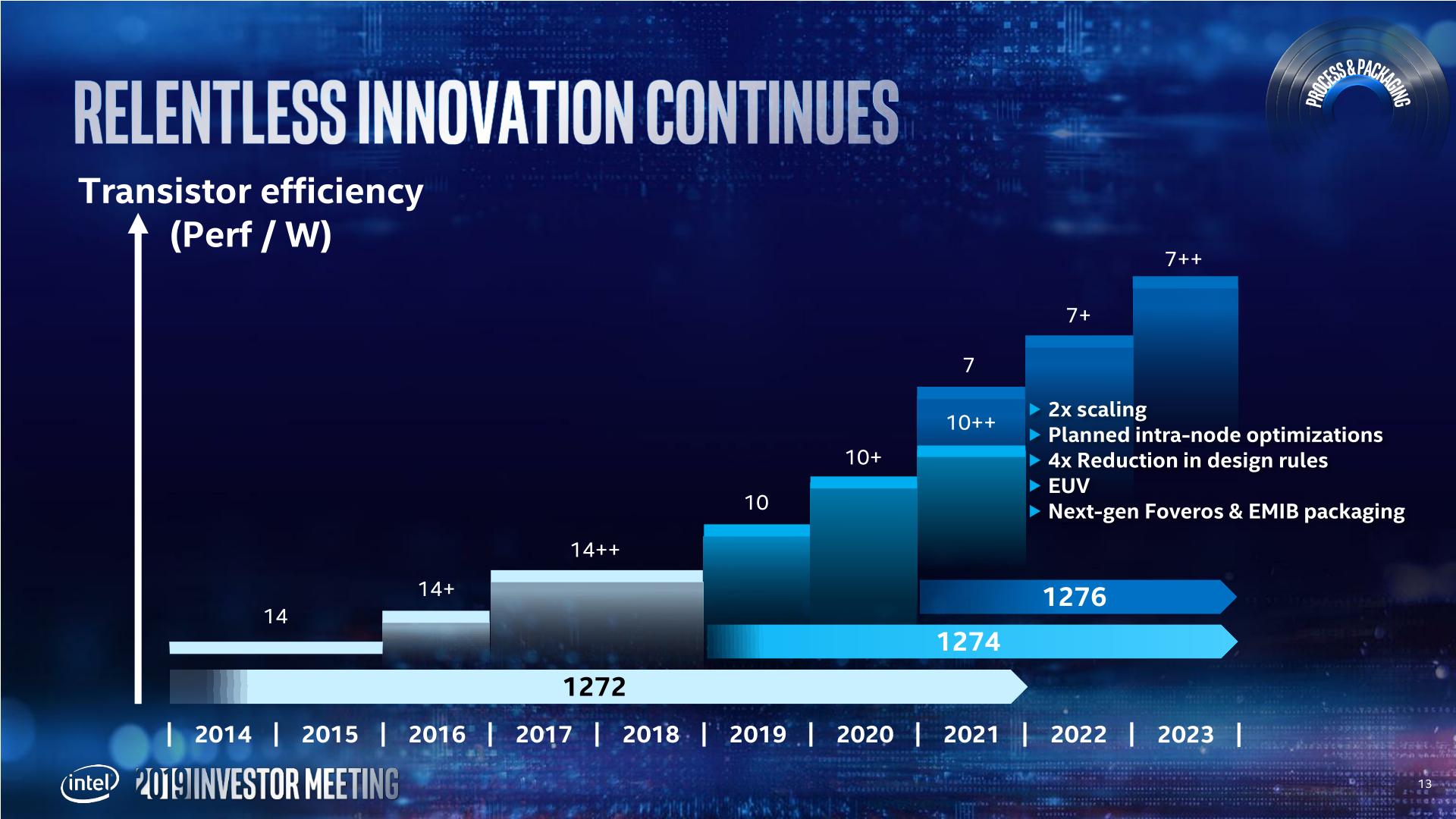
Intel’s first product to be made using its 7 nm manufacturing technology is its ‘big’ GPU for high performance computing that is due in Q4 2021, two years after the launch of the 10 nm Ice Lake CPU. Intel says that its 7 nm process is well on-track and the product will be released as planned. While Intel also plans to use 7+ and 7++ technologies in 2022 and 2023, the company is already working on its 5 nm process and is currently ‘engineering’ it, which means that the path-finding stage has been passed and fundamental things like materials and transistor structures were set.
Here is what Bob Swan, CEO of Intel, told analysts and investors on Thursday:
“We are on track to launch our first 7 nm based product, a datacenter-focused discrete GPU, in 2021, two years after the launch of 10 nm [products]. We are also well down the engineering path on 5 nm.”
Related Reading:
- Intel Begins Commercial Shipments of 10nm Ice Lake CPUs to OEMs
- The Ice Lake Benchmark Preview: Inside Intel's 10nm
- Examining Intel's Ice Lake Processors: Taking a Bite of the Sunny Cove Microarchitecture
- Intel Details Manufacturing through 2023: 7nm, 7+, 7++, with Next Gen Packaging
- Intel Process Technology Update: 10nm Server Products in 1H 2020, Accelerated 7nm in 2021
Source: Intel


59 Comments
View All Comments
Santoval - Monday, October 28, 2019 - link
"Fool me once, shame on me. Fool me twice..."It's actually the other way around ("Fool me once, shame on you. Fool me twice shame on me").
GreenReaper - Monday, October 28, 2019 - link
It shouldn't be acceptable for Intel to be fooling paying customers even once!twotwotwo - Monday, October 28, 2019 - link
(It's a call transcript where it's hard to get every comma right; maybe "server, storage, and network" was the intent?)Freeb!rd - Monday, October 28, 2019 - link
Those are usually lower core counts and lower speeds... 10nm Ice Lake Xeons are supposed to support PCIe 4.0 which you would want in server storage and networking. But if it won't show up until around the same time as Milan, will it have much impact?Scabies - Monday, October 28, 2019 - link
>We are on track to launch our first 7 nm based product, a datacenter-focused discrete GPU, in 2021Unless the thing gets Raja'd
Vitor - Monday, October 28, 2019 - link
LOL at 10++ being already mentioned.FreckledTrout - Monday, October 28, 2019 - link
"The company no longer sets ultra-ambitious goals for scaling each node, but attempts to find a right balance between performance, power, cost, and timing. "In other words Intel is copying TSMC's approach with 7nm. TSMC took a very low risk approach by only having some upfront process at 7nm and they didn't go to crazy on densities either. Sure the first 7nm process isn't spectacular but they have desktop chips on said process where Intel does not. So I would say very wise move to emulate TSMC's evolutionary instead of revolutionary approach as these nodes get more and more complex.
Kevin G - Monday, October 28, 2019 - link
More importantly, TSMC was able to ship and deliver what they promised for 7 nm roughly on time. They weren't as ambitious but that conservative design helped TSMC leap frog Intel's 10 nm.The real risk for TSMC's 7 nm node is the EUV variant. This actually simplifies some things (going to single patterning in some cases) but having the EUV tools ready for volume production was the greater variable. EUV has been a technology the entire fab business has been striving for the past decade. Kind of impressive that TSMC got to 7 nm without it.
FreckledTrout - Monday, October 28, 2019 - link
Pretty much my sentiment as well. I'm excited about TSMC's move to 7nm+ using EUV more than the first generation 7nm as this is where we really start to see 7nm shine. More so I expect to see decently higher clocks for AMD. We all see only one core able to hit those rated boost clocks for any given Zen2 CPU and its very obvious its TSMC's process holding that back. The quad patterning is obviously not extremely consistent albeit impressive they can do it at all.peevee - Monday, October 28, 2019 - link
" EUV more than the first generation 7nm as this is where we really start to see 7nm shine. More so I expect to see decently higher clocks for AMD."Why? It is a fabrication technology, how is it going to affect things like interference, leakage and resistance?