Intel's new Atom Microarchitecture: The Tremont Core in Lakefield
by Dr. Ian Cutress on October 24, 2019 1:30 PM EST
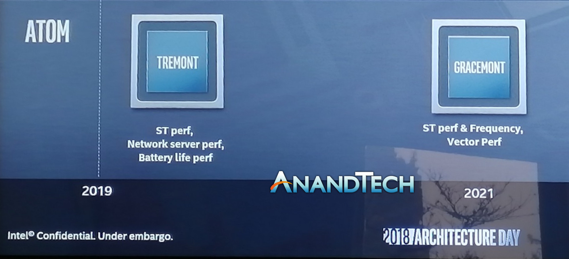
While Intel has been discussing a lot about its mainstream Core microarchitecture, it can become easy to forget that its lower power Atom designs are still prevalent in many commercial verticals. Last year at Intel’s Architecture Summit, the company unveiled an extended roadmap showing the next three generations of Atom following Goldmont Plus: Tremont, Gracemont, and ‘Future Mont’. Tremont is set to be launched this year, coming first in a low powered hybrid x86 design called Lakefield for notebooks, and using a new stacking technology called Foveros built on 10+ nm. At the Linley Processor Conference today, Intel unveiled more about the microarchitecture behind Tremont.
For the sake of clarity, a pre-note on ‘Core’ vs ‘core’:
- ‘Core’ and ‘Atom’ are Intel’s two main x86 microarchitecture families
- A ‘core’ is a single designated CPU capable of processing instructions, and can be built by Intel with either ‘Core’ or ‘Atom’ microarchitectures
A Brief History of Atom
Intel’s lower powered Atom microarchitecture has been used for a variety of solutions: embedded platforms, networking, smartphones, tablets, netbooks, NAS devices, control hubs, and a wide array of things we don’t even know about. The positioning of Atom compared to Core was meant to be that Atom was the smaller core design, taking up less silicon die area and being lower performance, but ultimately lower power in a time where the Core microarchitecture was focused more towards high performance designs.
The last few generations of Atom are readily quantified: Silvermont based on 22nm was a big product for the company, which has evolved into Airmont, Goldmont, Goldmont Plus, and now Tremont.
| Intel's Atom History | ||||||
| AnandTech | Node | Smartphone | Tablet | Netbook Notebook |
Networking Server |
|
| Saltwell | 32nm | 2011 | Medfield Clover Trail+ |
Clover Trail | Cedar Trail | |
| Silvermont | 22nm | 2013 | Merrifield Moorefield |
Bay Trail-T | Bay Trail-M Bay Trail-D |
Rangeley Avoton |
| Airmont | 14nm | 2015 | 'Riverton' | Cherry Trail-T | Braswell | Denverton |
| Goldmont | 14nm | 2016 | 'Broxton' | Willow Trail Apollo Lake |
Apollo Lake | |
| Goldmont+ | 14nm | 2017 | Gemini Lake | |||
| Tremont | 10+ | 2019 | Lakefield | Lakefield | Snow Ridge | |
The Atom family lines get a little confusing with Intel playing in all these spaces. The Atom core within in given family is usually identical (L2 configuration might change), and because of the SoC in play, it might get a different name based on the market where it was headed. Intel scrapped the smartphone program back with Broxton in 2016, and the tablet type of SoC has also gone away. With Lakefield, combining Core and Atom, it could be used in Tablets again for 2019/2020, but we will see it in Notebooks with the Surface Pro Neo and in networking/embedded markets as Snow Ridge.
Lakefield - 12mm x 12mm, 2mW Standby Power
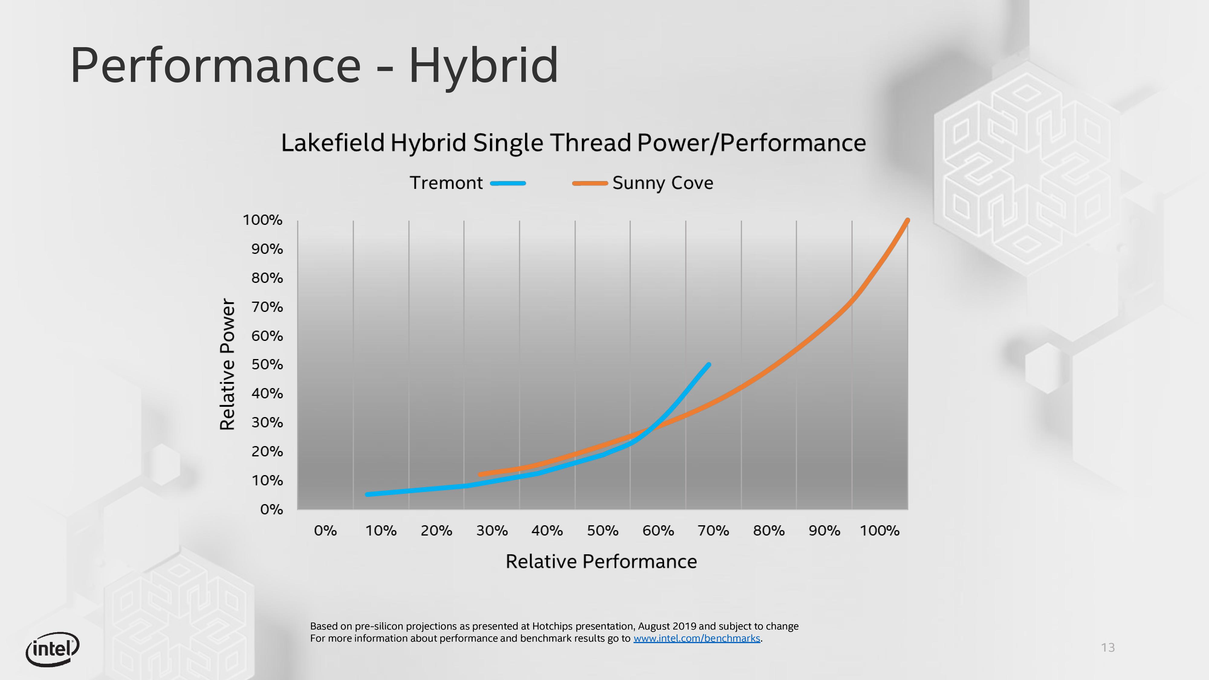
It is worth noting that as Intel expanded the scope of its Core microarchitecture, from 1.5W per core to 20W+ per core, it has kind of edged Atom more into niche products. Atom still had that super-low-power advantage, with a much smaller die area, but has also been super low performance with a quantifiable step-function below what Core can provide. With Tremont, Intel’s primary focus was bringing the single thread performance of the Atom design in parity to Core at the lower end of performance, with a sizeable overlap between the performance of a single Core design against a single Atom design. Intel published this graph to demonstrate what this looks like on early silicon:
Now, Intel’s Atom platforms haven’t had the greatest press over the last few years. Aside from providing some really nice notebooks around the $200 range on the consumer side, the enterprise side has been dealing with a clock degradation issue that ultimately leaves Atom systems built on C2000 processors unable to boot, which was bad news for embedded Atom systems designed to run for 10-20 years. Intel has since fixed that bug with a silicon update, but the point of that silicon was for it not to be touched for a generation.
With that aside, Intel is looking to revive its Atom fortunes with the new Tremont design, and looking forward to Gracemont and beyond. More performance, crossing over with Core, and with hardware built on Intel’s latest 10+ process, should afford a number of opportunities. Until we get our hands on the hardware, we’re going to examine the design.
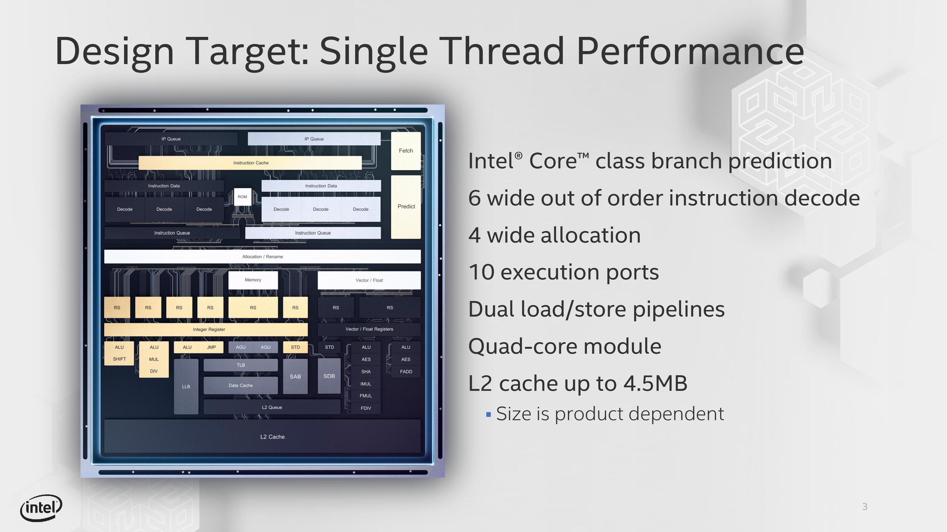
Design Goals for Tremont
The odd quirk about CPU design is that for engineers that have been embedded in this space for 20 years, when they were taught about processor design, the main focus was all about performance. Little attention was paid to power. Fast forward to today, and power is the often talked about point when it comes to battery powered devices, and learning to design for both performance and power becomes an intense balancing act for all the engineers involved. We’ve spoken to companies that only allow performance enhancements if the power increase is at most equal in percentage, or perhaps a 2:1 ratio of performance/power. It’s a difficult pie to bake at any rate.
The interesting thing here in our briefing with Intel is that they specifically stated that Tremont was built with performance in mind, and the aim was for a sizeable uptick in the raw clock-for-clock throughput compared to the previous generation Atom, Goldmont Plus. Based on Intel’s own metrics, namely using SPEC, Intel is going to claim an average 30% iso-frequency performance uplift in core performance for Tremont over Goldmont Plus.
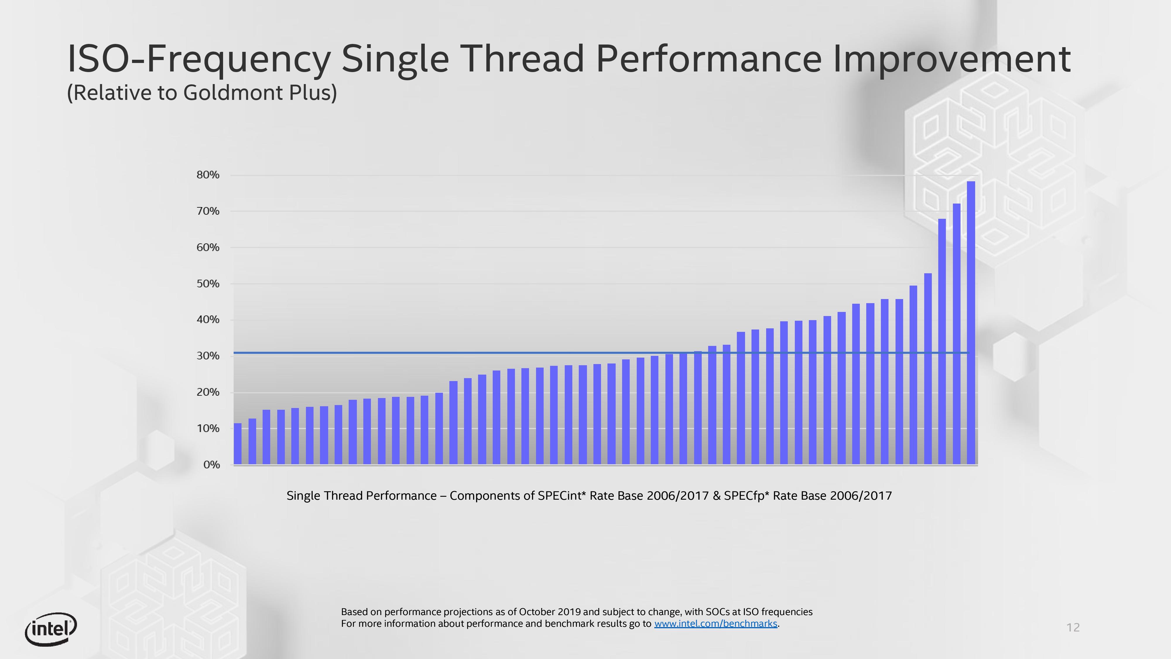
It’s worth noting here that this data is from an early Tremont design we were told, and should represent minimum uplifts. The graph is somewhat skewed at the top end with three of the SPEC tests getting 65%+ uplifts, and at the time of discussion, Intel did not have to hand exactly which tests these were (likely libquantum, lbm). We weren’t told how the code was compiled, however Intel did state that the same compiled binaries were used on both Tremont and Goldmont Plus. Intel didn’t state if they’re actually adjusting the clock of each core to match each other, or doing a performance per clock analysis using the frequency as a division factor. These results have to be taken at face value.
A 30% average jump in performance is a sizeable jump for any generation-to-generation cadence. Just taking it as-is feels premature: aside from microarchitectural advancements and a jump to 10nm, there has to be something at play here – either the power budget of Atom has ballooned, or the die area. With Intel explicitly out of the gate stating that their focusing on performance, a cynic is going to suggested that something else has paid that price, and to that end Intel wasn’t prepared to talk about power windows or die area, though they did point to the already announced Lakefield CPU, which has a 1 x Core + 4 x Tremont design and gets compared to 7 W CPUs.
Comparing 14nm Goldmont Plus (that’s standard 14nm, not 14+ or 14++) to a 10+ Tremont core is going to be difficult: the Tremont core has more in it to drive that performance, however what is not known is how much space was saved moving from 14nm to 10+ and if the extra parts make the core bigger or smaller overall. Needless to say, Tremont has more in it to drive that performance, which we’ll cover in the next few pages.


101 Comments
View All Comments
mode_13h - Saturday, October 26, 2019 - link
Yes, fadd is simply floating-point add. Same for fmul.What makes FMA "fused" is that the product isn't truncated before the accumulate, resulting in higher precision. So, what's "fused" is the multiplication and accumulation.
Fused-add or fused-multiply makes no sense - they each only do one thing, so what would you even be fusing?
The Hardcard - Thursday, October 24, 2019 - link
when I squint at the power/performance graph, I don’t see much of a power savings for Tremont. If that is 1.5 for Sunny, it looks like Tremont is will be more like 1 watt rather than 200mW. is it my eyes or are they being loose with the graph. also, it looks like performance drops much faster than power.Lakefield seems like it should be 2+4 rather than 1+4. it will be interesting to see how it compares to the 8cx for performance and battery life.
Santoval - Thursday, October 24, 2019 - link
In the graph Sunny Cove goes down to 12 - 13% "relative power" while Tremont reaches around 4 - 5%. So, if we assume a lowest of 13% relative power for Sunny Cove at 1.5W and a lowest of 4% for Tremont, this would suggest that Sunny Cove at its lowest power/frequency consumes 3.25 (13/4) times more power than Tremont at its lowest power/frequency.If that's indeed the case, and that graph is accurate, then Tremont consumes ~0.45 watts (1.5W / 3.25) at its lowest power, not 1 watt. However if that graph is only slightly inaccurate Tremont might really go down to 200mW operation mode. For instance if Sunny Cove's relative power was meant to terminate at 20% and Tremont's at 3% then their difference in power consumption at the lowest power mode is (20/3) 6.67 times, thus Tremont would go down to ~220mW.
The Hardcard - Thursday, October 24, 2019 - link
interesting, we both put Sunny at 12 percent. But my eyes put Tremont at 8 percent, which is how I got one watt. It just looks much closer to the 10 than the one. But, I assume Microsoft got figures that made sense to them so maybe you’re right.name99 - Friday, October 25, 2019 - link
We have to look at why this product exists. To me it looks like IBM's 8-way threading, ie a product of the decadent stage of CPU design, when the primary impulse becomes to game the markets rather than to optimize engineering metrics.Look at the performance/energy curve. There is SO MUCH overlap with Core. That makes little sense for a big.LITTLE type system -- if the primary goal is low power, you optimize the one core for low power, the other for performance, and make little effort to extend the low power performance beyond the lowest the high power core goes. (You want a small amount of overlap for hysteresis but not much more.) If you look at Apple's cores (which I know best) this is clear; the small cores max at about 30% of the performance of the large cores, and the large cores can clock down to about 1/3 maximum frequency.
But what if your goal is NOT primarily energy saving? The Tremont presentation talks a whole lot about performance, little (nothing that I saw) about where they saved energy and how much. What if your goal is to create a "reasonably powerful" lower end core, to at least good enough match current ARM AND to be able to expand your provision of multi-core (for PCs) and many-core (for laptops) without having to give up those nice juicy Core profits?...
Clearly you can think of Tremont as an A75 equivalent, to be sold to designs thinking of jumping ship at that performance level. But you can also view it as Intel's way of providing low-end laptops/desktops with 5 (or 6? who knows what the SMT situation of the large core is) threads without having to drop the prices on i5s. Likewise a way to compete with those 48 and 64-core lightweight ARMs (ThunderX, Cavium and suchlike) while again not having to drop the price of the large Xeons.
In this light, the omission of decent AVX is not a bug, it's a feature; it's one more reason that these are low class cores meant for peasants, while decent people should continue to pay for Cores.
On financial grounds, this may make sense, and Intels' plan is presumably to add AVX-512 when SVE becomes too common too ignore (but not until then...)
On strategic grounds does it make sense? Hmm.
- It may just prevent even more people from ever bothering to design, compile, and optimize for AVX. Maybe likewise for persistent memory? (That support seems pretty fragmented, and I'm sure Tremont won't help.)
- Even Intel isn't so large that they can keep creating substantially improved new designs every year (something that's become very clear over the past few years).
This particular fork seems to be one that doesn't allow for that much learning across the two teams (and may even lead to deliberate crippling if the Tremont direction gets "too" good).
Of course other design houses are even more opaque than Intel (I don't think we have any idea how much cross-learning there is between the ARM big and little core teams. Apple certainly APPEARS to have very good cross-learning [both the lock-step feature support and the very low performance overlap as minor pieces of evidence] but who can be sure?)
But they seem to have a better aligned set of incentives to keep everyone happy and in sync. (Team A goes for performance at this power level, team B for performance up to X and no further and this lower power level.)
Whereas Intel seems to be in the difficult situation (that VERY WIDE performance overlap range between the two cores) of "yeah, keep making it faster, but not too fast --- you'll know when you're too fast because we'll crush your spirit at that point..."
Anyway, lots of rambling here, but I think the key insight is to NOT see this as an ENERGY big.LITTLE play, regardless of what Intel says, but as a way to provide more cores at the low-end without hurting Core prices. (Of course there is still that pesky damn AMD forcing high-end Xeon prices to halve... Well, one battle at a time.)
Namisecond - Friday, November 1, 2019 - link
8cx will probably beat Lakefield in terms of efficiency, but Lakefield has native x86 and probably better perceived performance.azfacea - Thursday, October 24, 2019 - link
wrong title. this aint new. its pentium 4 shrink/rebrandJorgp2 - Thursday, October 24, 2019 - link
Lol, norozquilla - Thursday, October 24, 2019 - link
I love my J5005 (Gemini Lake) as an HTPC, and I lent it to a relative for a while after his AMD A10-7860K (Piledriver, meh...) failed, he felt it worked around the same, and faster on videos...Which is why I love this CPU, it is fanless and stays at around ~8W and plays back 10bit 4K content in my living room TV without any issues. I also added a CNVI 802.11ac module, it performs great.
Hopefully this Tremont Core will provide something like that, but I will upgrade until there is AV1 hardware decoding. With which GPU will it be paired, a Gen11 something? I think AV1 is still a bit down the road with x86, ARM already has a couple of proposals.
For day to day office and HTPC duties, I haven't found a better alternative (maybe RPi4 in this segment?), I'm also waiting to see the Ryzen embedded alternatives for home use, so far only expensive industrial-ish options.
GreenReaper - Thursday, October 24, 2019 - link
Usually the video block is shared across all segments, so if the APU form of Navi picks up AV1 support, chances are it'll be available. Might be a while until truly low-end APUs are available, though.