SMIC: 14nm FinFET in Risk Production; China's First FinFET Line To Contribute Revenue by Late 2019
by Anton Shilov on August 16, 2019 3:00 PM EST- Posted in
- Semiconductors
- 14nm
- FinFET
- SMIC
SMIC, the largest contract maker of semiconductors in China, announced this month that it would start commercial production of chips using its 14 nm FinFET manufacturing technology by the end of the year. This is the first FinFET manufacturing line in China, making it a notable development for a country that already houses a significant number of fabs, as the world's leading-edge manufacturers never installed FinFET technology in China for geopolitical and IP reasons. SMIC in turn seems to expect a rather rapid ramp of its 14 nm node, as it anticipates the new manufacturing line will meaningfully contribute to its revenue before the end of the year.
According to SMIC, their 14 nm FinFET manufacturing technology was developed entirely in-house and is expected to significantly increase transistor density, increase performance, and lower power consumption of chips when compared to devices made using the company’s 28 nm process that relies on planar transistors. Earlier this year it was expected that SMIC would start production of 14 nm chips already in the first half of 2019, so the firm seems to be a little behind the schedule. Nonetheless, an in-house FinFET process technology is quite a breakthrough for a relatively small company that puts it into a club with just five other foundries with FinFET technologies.
One interesting thing that SMIC said about its 14 nm FinFET volume ramp is that it expects the process to have a significant revenue contribution already by the end of the year. Meanwhile, keeping in mind that right now SMIC only has two relatively small 300-mm HVM fabs (which are currently used for 28 nm – 65 nm nodes) that are heavily utilized generating 40 ~ 49% of the company’s revenue (in Q1/Q2 2019), it is difficult to imagine SMIC making loads of 14 nm chips in 2019.
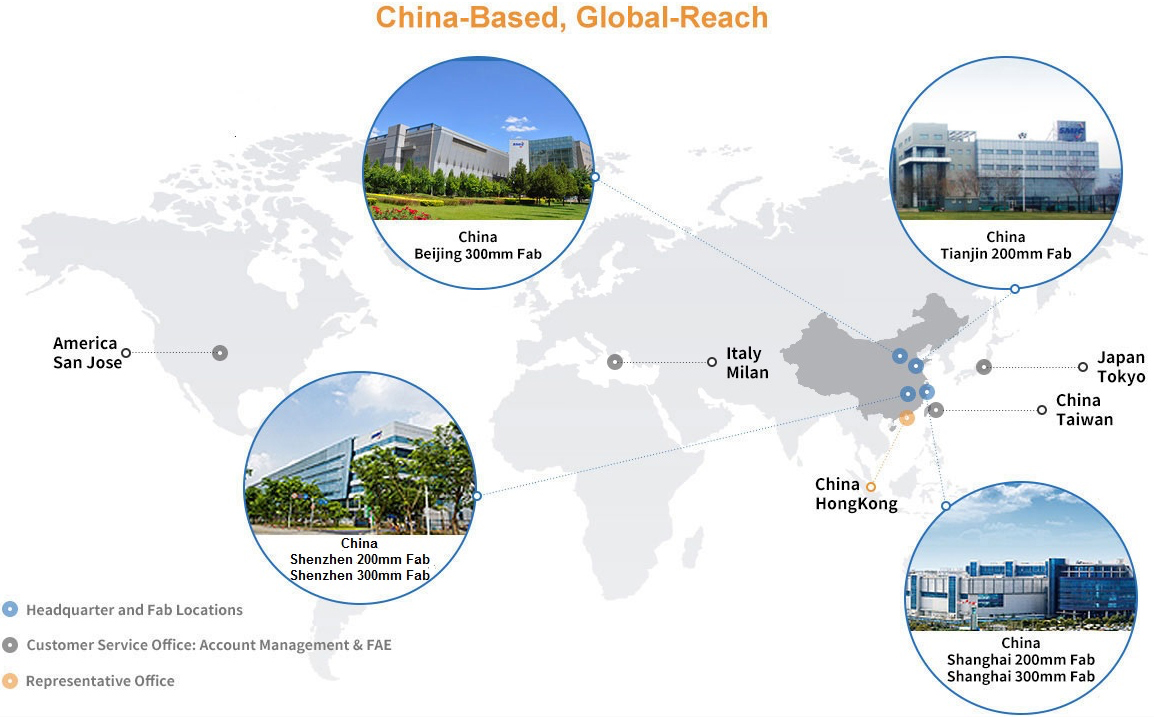
| Overview of SMIC's Fabs | ||||
| Process Technologies | Capacity Wafer Starts per Month |
Location | ||
| BJ | 200mm | 90 nm - 150 nm | 50,000 | Beijing, China |
| 300mm | 28 nm - 65 nm | 35,000 | ||
| SH | 200 mm | 90 nm - 350 nm | 120,000 | Shanghai ,China |
| 300 mm | 28 nm - 65 nm | 20,000 | ||
| SZ | 200 mm | 90 nm - 350 nm | 60,000 | Shenzhen, China |
| 300 mm | 28 nm - 65 m | 3,000 | ||
| TJ | 200 mm | 90 nm - 350 nm | 50,000 | Tianjin, China |
| LF | 200 mm | 90 nm - 180 nm | 50,000 | Avezzano, Italy |
Earlier this year the company completed construction of its $10 billion SMIC South FinFET Fab, which will be used for its leading-edge manufacturing technologies and began moving in the equipment. Once the fab is ready for commercial operations, SMIC will be able to considerably increase production of chips using its 14 nm and then 12 nm FinFET fabrication technologies.
SMIC’s longer-term plans include 10 nm and 7 nm manufacturing processes. The latter is expected to require usage of extreme ultraviolet lithography tools, so last year SMIC acquired an EUV step-and-scan system from ASML for $120 million, which was to be delivered in 2019.
Related Reading:


53 Comments
View All Comments
Alexvrb - Sunday, August 18, 2019 - link
What? No way... Shabby may have made an ignorant comment rooted in what he recalled about AMD from over a decade ago, but there's NO comparison to Phynaz.Santoval - Saturday, August 17, 2019 - link
Did you think you time traveled 10+ years to the past or are you trying to live up to your username? AMD no longer has a fab, and they haven't technically had one since 2009 that they span off their fab business as GlobalFoundries (GF). At that time AMD had a 34% stake in GF. In 2012 they sold their last ~9% share in GF, so since that time AMD is completely out of the fab business, with not even a small minority share in a fab.dullard - Monday, August 19, 2019 - link
Fabs have nothing to do with it. If they produce a usable CPU, in China, at low Chinese prices, who then in Asia or Africa would buy AMD's CPUs? Why pay more unless AMD makes a highly compelling non-price based market niche for themselves?Jorgp2 - Friday, August 16, 2019 - link
Now we just need AMD to do the sameIronchef3500 - Monday, August 19, 2019 - link
:)Sychonut - Friday, August 16, 2019 - link
Looking forward to their 14++++++ offerings.webdoctors - Friday, August 16, 2019 - link
Is 14nm Finfet equivalent to say 12nm at TSMC or equivalent to 28nm at TSMC?Not sure if everyone uses the same sizing terminology. 14nm seems amazing, MOST companies don't need the latest/greatest node, i.e. 5nm or 7nm. There's 100s of fabless chip design companies and outside of Qualcomm/Apple/Intel/Nvidia/AMD, most will love another cheap alternative to the bigname fabs.
Should really help bring down BOM costs for pretty much everyone, from ICs in HDDs, TVs , tablets to cars.
ksec - Saturday, August 17, 2019 - link
Not 12nm, not even 16nm. ( TSMC's 12nm is basically TSMC's 16nm+++, they can't use 14nm due to how it rhymes with the word Dead in Chinese )The 14nm will be similar or even worst than Smasung's first 14nm, but still likely to be better than TSMC's 20n.m Not sure if that answer your question.
levizx - Monday, August 19, 2019 - link
Funny you mention that, seeing the actual Chinese foundry is using what can't be used.Azethoth - Friday, August 16, 2019 - link
Neat, developed "entirely in house" by their hacking and industrial espionage group!