Intel Details Manufacturing through 2023: 7nm, 7+, 7++, with Next Gen Packaging
by Ian Cutress & Anton Shilov on May 8, 2019 4:35 PM EST
At Intel's Investor Day today, CEO Bob Swan and Murthy Renduchintala spoke to the ability of the company with respect to its manufacturing capabilities. Intel has historically been strong in its ability to execute on its process technology, however the delay of its 10nm process has obviously raised multiple question marks, and has done for several years. The two Intel executives went into a little detail about what Intel was doing in the interim, and how it has learned from the issues.

Back in 2013, Intel envisoned its 10nm to succeed the 14nm by providing 2.7x density, with new technologies such as Self-Aligned Quad Patterning (SAQP), Contact over Active Gate (COAG), Cobolt Interconnects, and new packaging technologies such as EMIB and Foveros. Intel admits that this was an ambitious plan, and the goals were not clearly defined with the teams and it was ultimately overly complex and not managed in an ideal way.
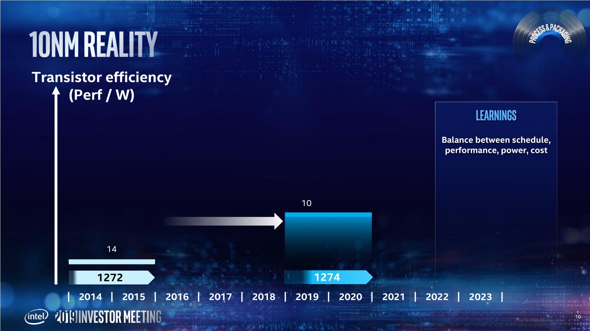
This ended up pushing 10nm out into a later time frame. In this case, Intel pushed 10nm out to 2019 (technically they shipped Cannon Lake in small quantities on 10nm in 2017, however that is nothing more than a curio in the timeline of semiconductors), and filled the gap with 14+ and 14++.

Intels 14+ and 14++ processes extracted more than 20% more performance (from Broadwell to Whiskey Lake) from the process since its inception. As a result, Intel is prepared to not only get ready for future intra-node optimizations, but actually adjust the roadmap to compensate for it. Murthy made it clear that Intel wants to introduce a Moore's Law-like gain at the beginning of a new process, and another similar gain by the end of the process.
Intel has stated that its 10nm product family (beyond Cannon Lake) will start to be available from the middle of this year (2019), with Ice Lake on client platforms (notebooks).

Intel will be launching multiple 10nm products through 2019 and 2020, including server based 10nm in the first half of 2020:
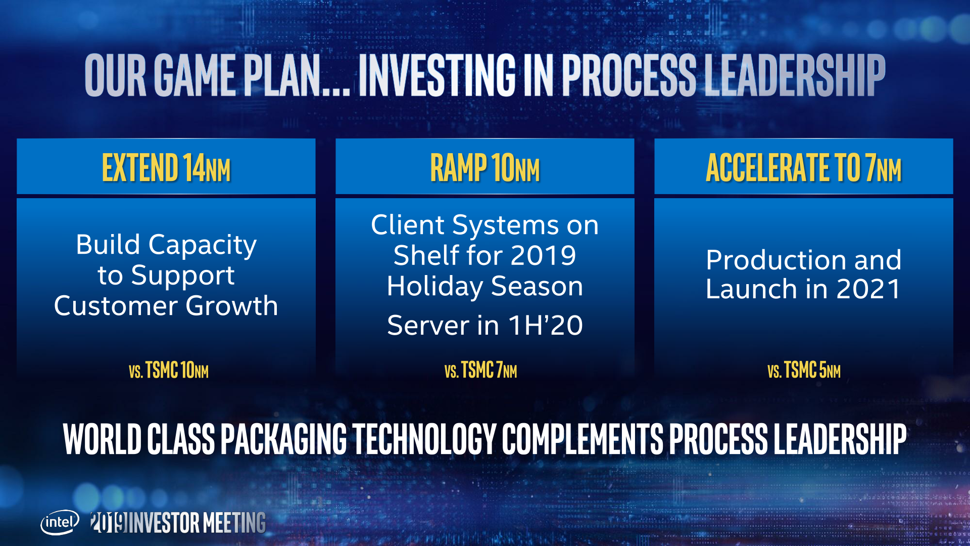
In the above slide, Intel states that it will have 7nm in production and launching a product in 2021. That sounds very aggressive for a company that has had issues with 10nm. It even shows in Intels radmap, with 10nm (and 10+ and 10++) having a much shorter life cycle than the 14nm family of processes.
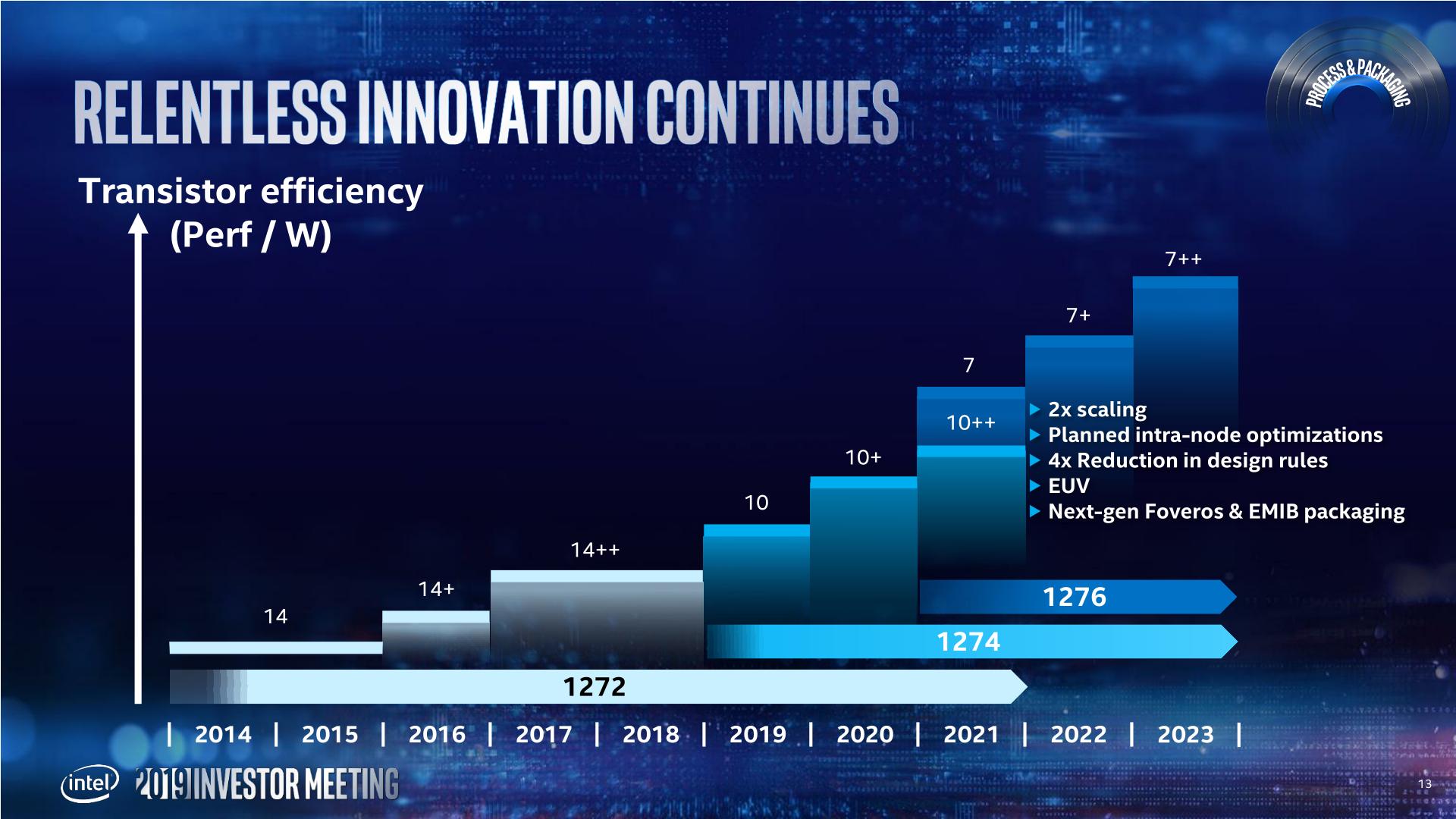
With this in mind, Intel's 7nm is going to be the combination of what Intel has learned from the 14nm and 10nm family of products. Intel wants that 2x scaling (Moores Law), but with intra-node optimations planned as part of the roadmap. Intel is also reducing its number of design rules, which should help with execution. 7nm will also be where Intel intersects with EUV, and also introduce next-gen Foveros and EMIB packainging.
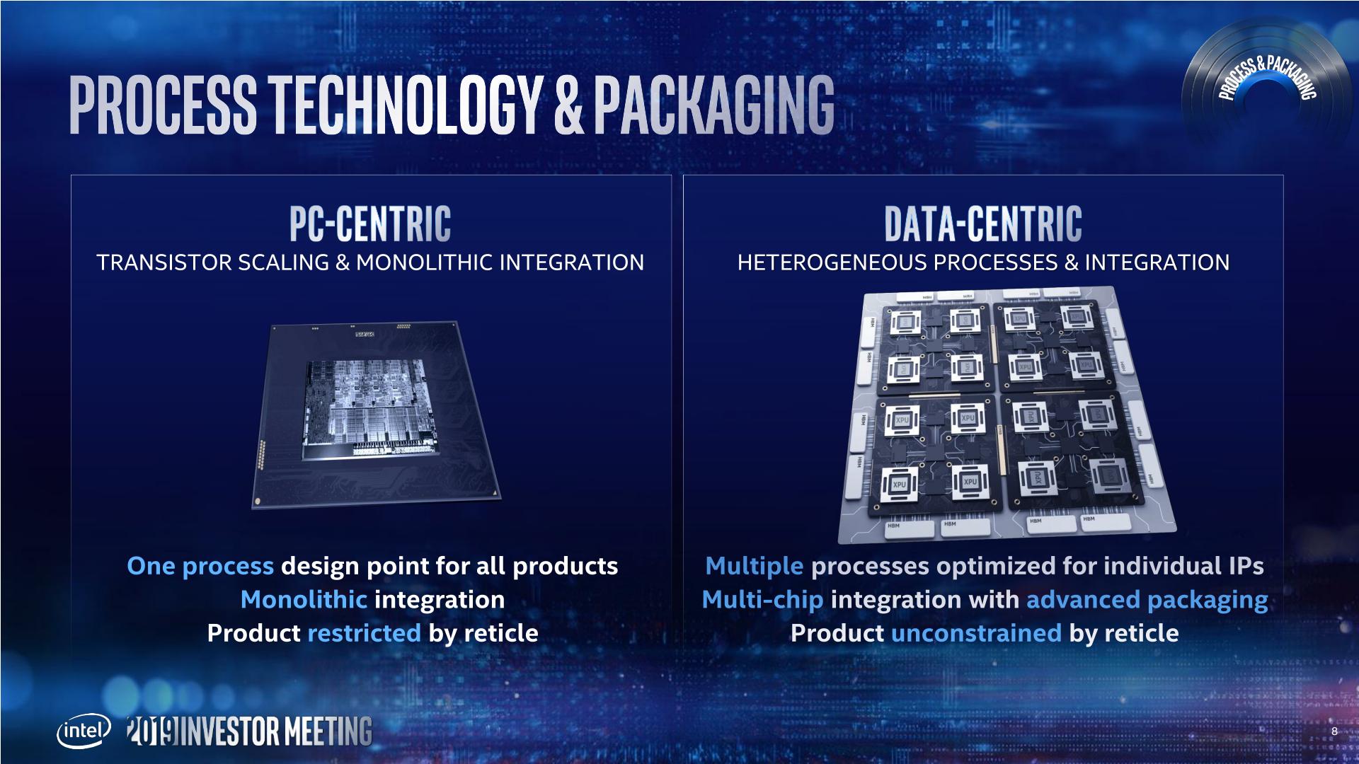
Intel provided this slide, which shows a monolithic PC-Centric die with a multi-die Data-Centric chip built on both Foveros and EMIB. This corroborates our discussion with Intel's chiplet and packaging team, who also stated that we would see Foveros and EMIB on a combined product - specifically the GPU.

Intel announced that its lead 7nm product (lead = top, or lead = first?) would be its new GPGPU, built on the Xe graphics architecture. Intel has stated that its Xe product stack will feature two different microarchitectures from mobile client up to GPGPU, with one of those architectures called Arctic Sound - technically Intel will launch its first discrete GPU in 2020 according to its press release, however the 7nm GPGPU will be launched in 2021.
More information is coming out of Intel's Event, more to follow.
Related Reading
- Intel: EUV-Enabled 7nm Process Tech is on Track
- Intel Starts Qualification of Ice Lake CPUs, Raises 10nm Volume Expectation for 2019
- Intel Agilex: 10nm FPGAs with PCIe 5.0, DDR5, and CXL
- Intel to Equip Fab 42 for 7 nm
- Intel Discloses Plans to Spend $5 Billion on Fab 28 Expansion in Israel
- Intel Submits Ireland Fab Expansion Plan: $8 Billion Price Tag, With a 4 Year Lead Time
- Intel Details Plans for Its Oregon Fab Expansion: D1X Phase 3
- Intel to Expand Production Capacities at Multiple Fabs
Source: Intel


237 Comments
View All Comments
Zizy - Thursday, May 9, 2019 - link
GPUs are always denser than CPUs for a variety of reasons, but yeah, TSMC does have very high density in actual products, while Intel's (and previous AMD's or IBM's) chips have much lower density than what the process could perhaps somewhat be capable of.Santoval - Thursday, May 9, 2019 - link
CPU cache is not the most dense, it is the *least* dense part of a chip. That's due to SRAM's 6 transistors per cell, which is the most frequent SRAM structure. DRAM, by contrast, is much denser.name99 - Thursday, May 9, 2019 - link
Since DRAM is not present on the chips in question, the relevance of your point is unclear...Hell, why not go all in and complain that SRAM is less dense than flash?
Santoval - Thursday, May 9, 2019 - link
DRAM has been often used for CPUs with L4 cache in the form of eDRAM. Intel makes such CPUs, IBM also makes them. I hope the relevance is more clear now.peevee - Thursday, May 9, 2019 - link
Even in these rare cases, DRAM is not on the same chip.Zizy - Thursday, May 9, 2019 - link
You are mixing storage and transistor density here. SRAM is not dense in capacity/mm but it is dense in transistors/mm.Santoval - Thursday, May 9, 2019 - link
You are technically right, however since we are talking about CPU *caches* their effective density (how many transistors are required for each KB) is important. Transistors for logic are different, since you can't easily quantify logic transistors with a simple KB or MB number. Logic is .. quite more complex.The comment of Wilco I replied to mentioned that "CPU cache is the densest part of the CPU". Densest in what sense? CPU caches waste a huge amount of die space, and millions of transistors merely for up to a few MB of cache. That doesn't sound remotely "dense" to me.
Wilco1 - Thursday, May 9, 2019 - link
No - caches are significantly more dense than logic. Denser both in the sense of transistors per area as well as bits/area due to being extremely tightly packed and repeated millions of times. Logic wastes a lot of area due to being irregular and all the routing required.DRAM is denser than SRAM on a per-bit basis, and flash is much denser again. But that's irrelevant to this discussion given only IBM uses eDRAM.
psychobriggsy - Thursday, May 9, 2019 - link
I think he was trying to say that you can have lower density SRAM - however this is only used in register files and L0/L1 caches in the performance critical areas.That goes the other way too. IBM was using eDRAM as on-die L4 cache for density reasons.
Smell This - Thursday, May 9, 2019 - link
Short cell libraries are optimized for high density and low power, and is 70% +/- of graphics and 'uncore' of the die size.I think 'cache' cell libraries are much less dense, more power 'hungry" and optimized for speed.