Intel Details Manufacturing through 2023: 7nm, 7+, 7++, with Next Gen Packaging
by Ian Cutress & Anton Shilov on May 8, 2019 4:35 PM EST
At Intel's Investor Day today, CEO Bob Swan and Murthy Renduchintala spoke to the ability of the company with respect to its manufacturing capabilities. Intel has historically been strong in its ability to execute on its process technology, however the delay of its 10nm process has obviously raised multiple question marks, and has done for several years. The two Intel executives went into a little detail about what Intel was doing in the interim, and how it has learned from the issues.
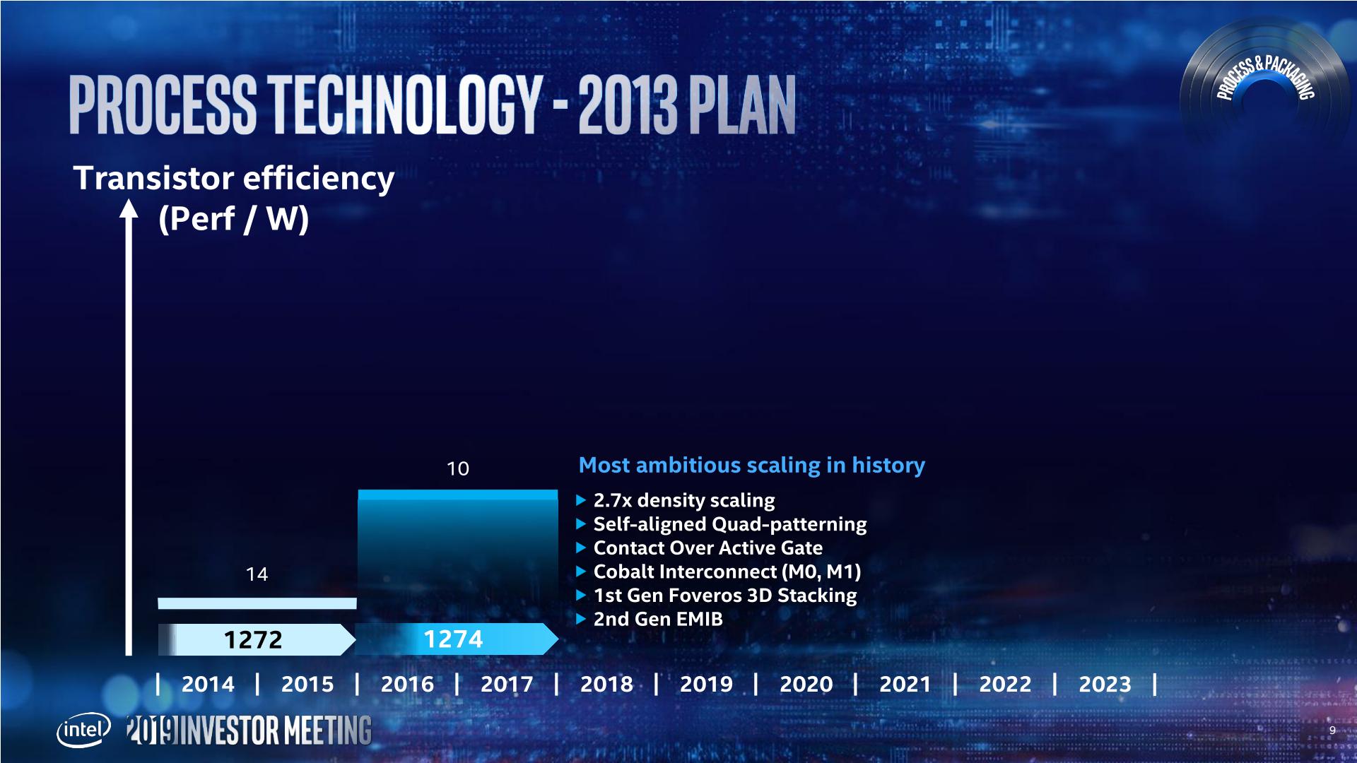
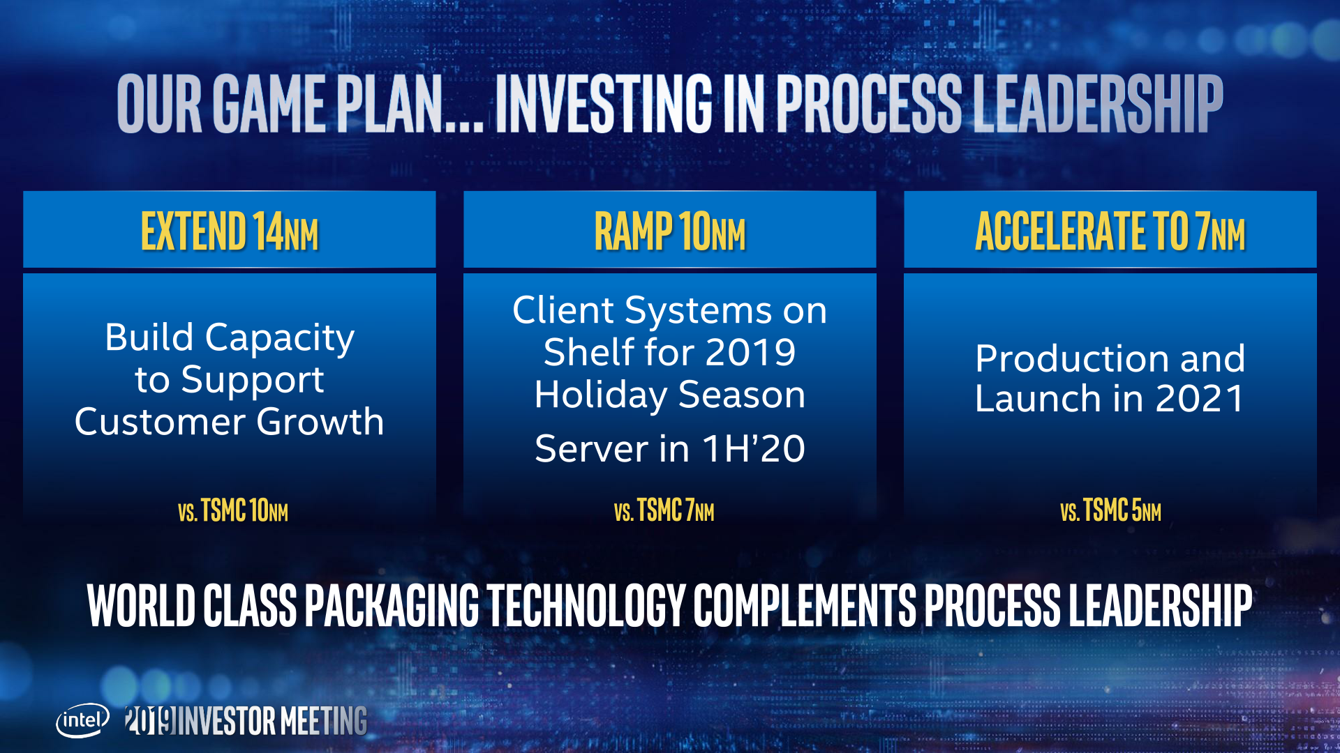
Back in 2013, Intel envisoned its 10nm to succeed the 14nm by providing 2.7x density, with new technologies such as Self-Aligned Quad Patterning (SAQP), Contact over Active Gate (COAG), Cobolt Interconnects, and new packaging technologies such as EMIB and Foveros. Intel admits that this was an ambitious plan, and the goals were not clearly defined with the teams and it was ultimately overly complex and not managed in an ideal way.
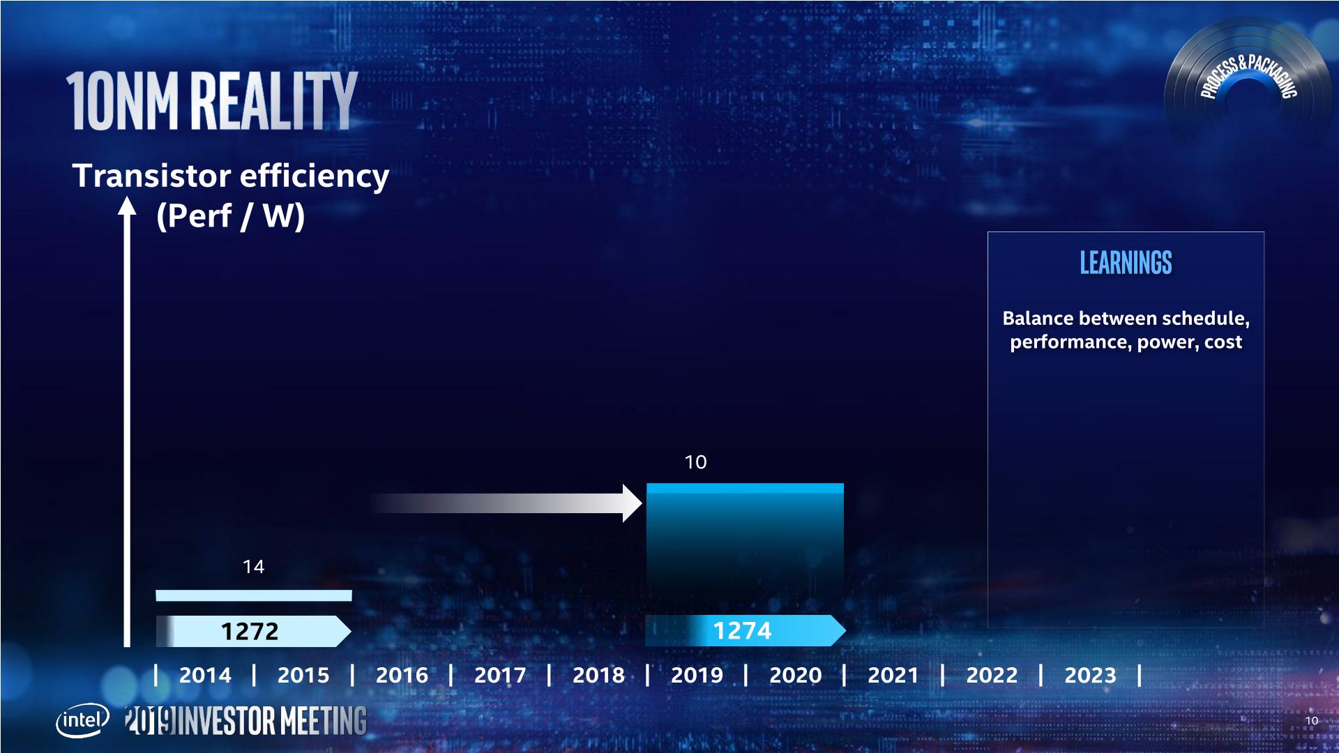
This ended up pushing 10nm out into a later time frame. In this case, Intel pushed 10nm out to 2019 (technically they shipped Cannon Lake in small quantities on 10nm in 2017, however that is nothing more than a curio in the timeline of semiconductors), and filled the gap with 14+ and 14++.
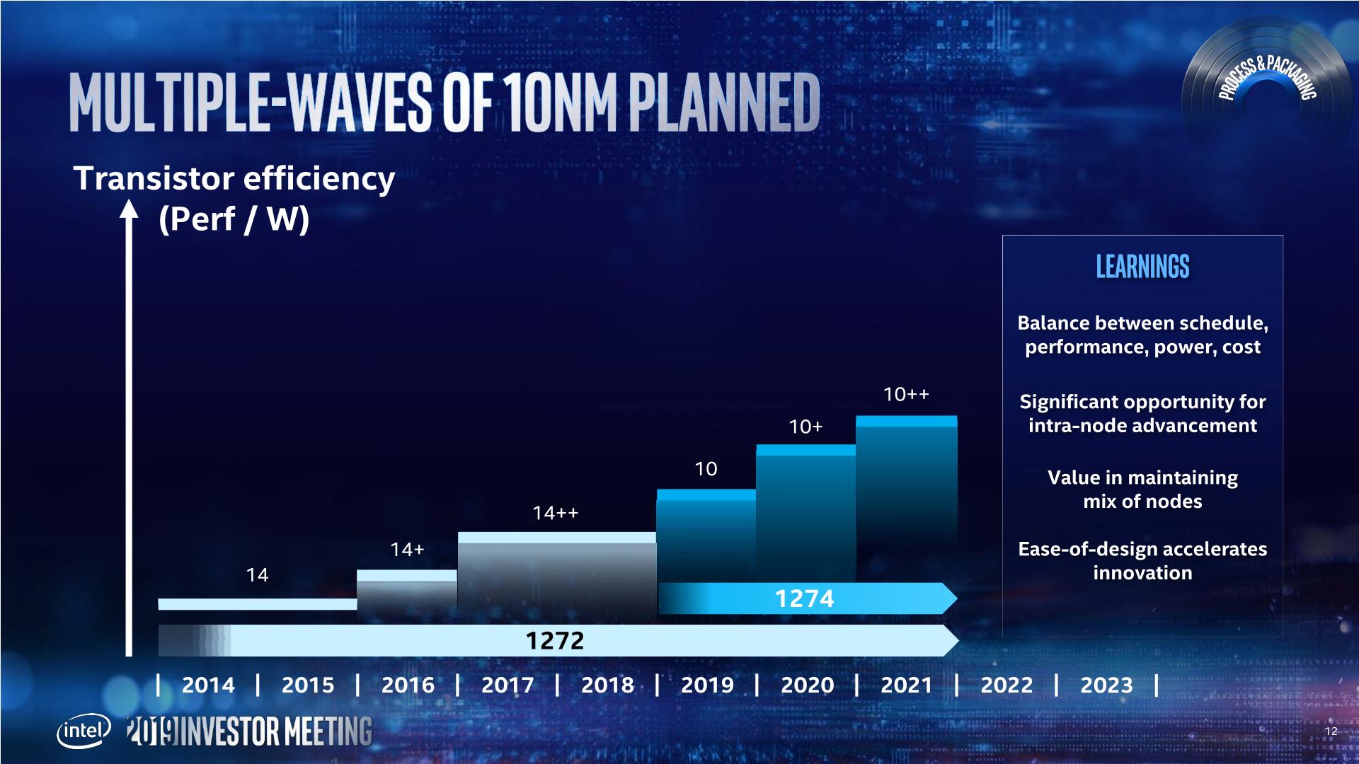
Intels 14+ and 14++ processes extracted more than 20% more performance (from Broadwell to Whiskey Lake) from the process since its inception. As a result, Intel is prepared to not only get ready for future intra-node optimizations, but actually adjust the roadmap to compensate for it. Murthy made it clear that Intel wants to introduce a Moore's Law-like gain at the beginning of a new process, and another similar gain by the end of the process.
Intel has stated that its 10nm product family (beyond Cannon Lake) will start to be available from the middle of this year (2019), with Ice Lake on client platforms (notebooks).

Intel will be launching multiple 10nm products through 2019 and 2020, including server based 10nm in the first half of 2020:
In the above slide, Intel states that it will have 7nm in production and launching a product in 2021. That sounds very aggressive for a company that has had issues with 10nm. It even shows in Intels radmap, with 10nm (and 10+ and 10++) having a much shorter life cycle than the 14nm family of processes.
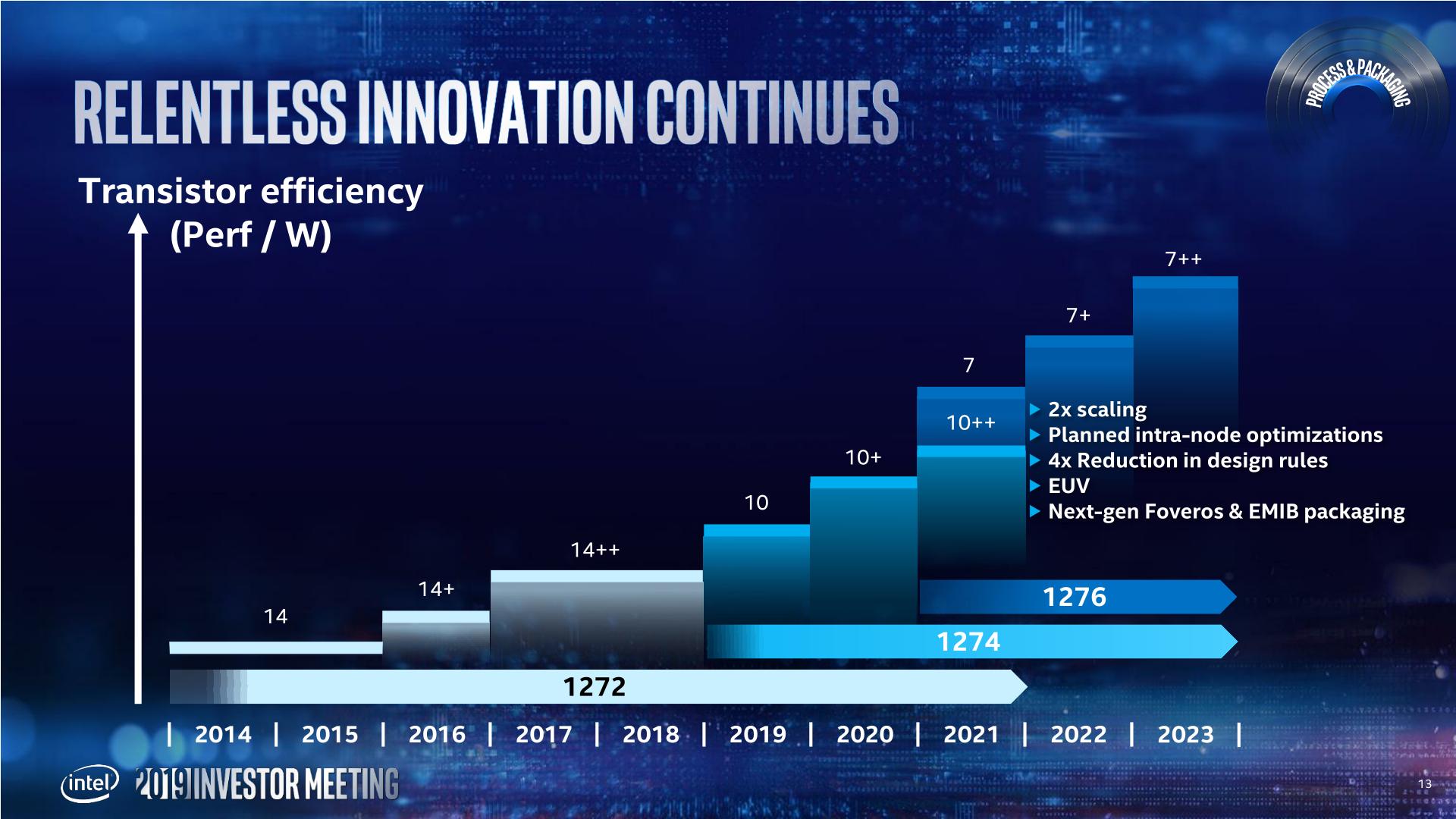
With this in mind, Intel's 7nm is going to be the combination of what Intel has learned from the 14nm and 10nm family of products. Intel wants that 2x scaling (Moores Law), but with intra-node optimations planned as part of the roadmap. Intel is also reducing its number of design rules, which should help with execution. 7nm will also be where Intel intersects with EUV, and also introduce next-gen Foveros and EMIB packainging.
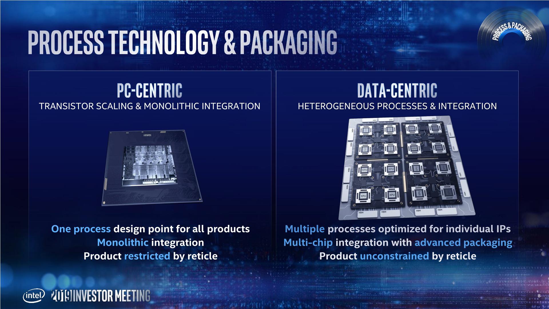
Intel provided this slide, which shows a monolithic PC-Centric die with a multi-die Data-Centric chip built on both Foveros and EMIB. This corroborates our discussion with Intel's chiplet and packaging team, who also stated that we would see Foveros and EMIB on a combined product - specifically the GPU.

Intel announced that its lead 7nm product (lead = top, or lead = first?) would be its new GPGPU, built on the Xe graphics architecture. Intel has stated that its Xe product stack will feature two different microarchitectures from mobile client up to GPGPU, with one of those architectures called Arctic Sound - technically Intel will launch its first discrete GPU in 2020 according to its press release, however the 7nm GPGPU will be launched in 2021.
More information is coming out of Intel's Event, more to follow.
Related Reading
- Intel: EUV-Enabled 7nm Process Tech is on Track
- Intel Starts Qualification of Ice Lake CPUs, Raises 10nm Volume Expectation for 2019
- Intel Agilex: 10nm FPGAs with PCIe 5.0, DDR5, and CXL
- Intel to Equip Fab 42 for 7 nm
- Intel Discloses Plans to Spend $5 Billion on Fab 28 Expansion in Israel
- Intel Submits Ireland Fab Expansion Plan: $8 Billion Price Tag, With a 4 Year Lead Time
- Intel Details Plans for Its Oregon Fab Expansion: D1X Phase 3
- Intel to Expand Production Capacities at Multiple Fabs
Source: Intel


237 Comments
View All Comments
Smell This - Thursday, May 9, 2019 - link
I continue to believe that originally cell libraries at 10nm were dinked, and the Chipzillah 14nm "Process-Architecture-Optimization' further went crapola. AMD 28nm SHP 'Excavator' cell libraries were/are comparable to 14nm, and certainly less dense than Kaby 14nm+ and subsequent optimizations.I think the standard high-density libraries from 14nm to 10nm are 20-33% "less dense" depending upon block/tool mods.
Wilco1 - Wednesday, May 8, 2019 - link
Also Intel CPUs traditionally only achieve a small fraction of the maximum theoretical density. For example Kirin 980 has ~93 million transistors/mm^2, while a 14nm Xeon achieves just 15.8 million transistors/mm^2.So 7nm TSMC is a whopping 6 times more dense, and that despite Xeon having significantly more cache (which is the most dense). Even if Intel 10nm delivers its original promise, it will still be more than 2 times off TSMC 7nm.
peevee - Wednesday, May 8, 2019 - link
It's original promise was over 100 MT/mm2 in a balanced SRAM/logic combo. It's to be seen what it is actually going to be in volume parts.But judging from "10nm", if their "7nm" volume production to be expected in 2021, pilot production should be happening now, and it is nowhere in sight. Meanwhile TSMC starts volume on EUV "7+" and "6nm" very soon.
I wish at least press would switch from those fake "nm" to MT/mm2 x GHz (SRAM or 50/50 or 60/40, does not really matter as long as it is common), we all be talking on much more real, physical level, amd not this marketoidal BS.
Wilco1 - Wednesday, May 8, 2019 - link
TSMC 7+nm is already in production. TSMC 5nm started risk production a while ago with volume production next year - that means 7+nm iPhones this year and 5nm next year.Even the MT/mm^2 are easy to manipulate by giving numbers for a low-track library which isn't useful in the real world. Hence my point that Intel doesn't ever get anywhere near the claimed densities for their processes. They specifically invented their density metric as that was the only way 10nm looked competitive with TSMC 7nm. However TSMC has shipped hundreds of millions of chips with 90+ MT/mm^2. Let's see when Intel ships a single one that does 90 MT/mm^2.
peevee - Thursday, May 9, 2019 - link
"TSMC 7+nm is already in production."Note I wrote "volume", not "production". What volume products are on 7+ now?
Wilco1 - Thursday, May 9, 2019 - link
Next iPhone is said to use 7+nm. That means full scale production right now to get 50+ million units fabbed.peevee - Tuesday, May 14, 2019 - link
Phone which will be released in 4.5 months? Pure speculation about the volume production yet.levizx - Friday, May 10, 2019 - link
Kirin 985/990 and A13 are in volume production now. Otherwise TSMC won't be able to ship the chip before August for a October consumer device launch.peevee - Thursday, May 9, 2019 - link
"Even the MT/mm^2 are easy to manipulate by giving numbers for a low-track library which isn't useful in the real world."As long as it is the same thing, the metric is still infinitely more useful than completely misleading "nm". Even pure SRAM would be useful all by itself as caches have to take a lot of space on 5GHz parts.
Also note I wrote "x GHz" there. Of course it is much much easier to make dense 1-2GHz than 5GHz. I suspect it is what is happening to Intel's "10 nm" now - they will have 2GHz Y (and maybe U) mobile parts and Xeons, not 5GHz desktop parts.
wumpus - Thursday, May 16, 2019 - link
Only the L1 cache really needs to operate at 5GHz (the L2 will probably be pretty close as well). By the time you get out to L3 or so, the densities should be comparable.High density 6T SRAM is likely to be the best way to compare density (even if the "good stuff" is 7.5T).