NVIDIA Announces the GeForce RTX 20 Series: RTX 2080 Ti & 2080 on Sept. 20th, RTX 2070 in October
by Ryan Smith on August 20, 2018 4:00 PM EST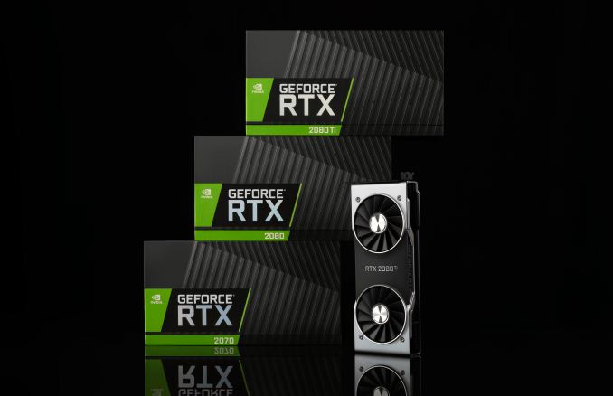
NVIDIA’s Gamescom 2018 keynote just wrapped up, and as many have been expecting since it was announced last month, NVIDIA is getting ready to launch their next generation of GeForce hardware. Announced at the event and going on sale starting September 20th is NVIDIA’s GeForce RTX 20 series, which is succeeding the current Pascal-powered GeForce GTX 10 series. Based on NVIDIA’s new Turing GPU architecture and built on TSMC’s 12nm “FFN” process, NVIDIA has lofty goals, looking to drive an entire paradigm shift in how games are rendered and how PC video cards are evaluated. CEO Jensen Huang has called Turing NVIDIA’s most important GPU architecture since 2006’s Tesla GPU architecture (G80 GPU), and from a features standpoint it’s clear that he’s not overstating matters.
As is traditionally the case, the first cards out of the NVIDIA stable are the high-end cards. But in a rather sizable break from tradition we’re not only going to get the x80 and x70 cards at launch, but also the x80 Ti card as well. Meaning the GeForce RTX 2080 Ti, RTX 2080, and RTX 2070 will all be hitting the streets within a month of each other. NVIDIA’s product stack is remaining unchanged here, so RTX 2080 Ti remains their flagship card, while RTX 2080 is their high-end card, and then RTX 2070 the slightly cheaper card to entice enthusiasts without breaking the bank.
All three cards will be launching over the next two months. First off will be the RTX 2080 Ti and RTX 2080, which will launch September 20th. The RTX 2080 Ti will start at $999 for partner cards, while the RTX 2080 will start at $699. Meanwhile the RTX 2070 will launch at some point in October, with partner cards starting at $499. On a historical basis, all of these prices are higher than the last generation by anywhere between $120 and $300. Meanwhile NVIDIA’s own reference-quality Founders Edition cards are once again back, and those will carry a $100 to $200 premium over the baseline pricing.
Unfortunately, NVIDIA is already taking pre-orders here, so consumers are essentially required to make a “blind buy” if they want to snag a card from the first batch. NVIDIA has offered surprisingly little information on performance and we’d suggest waiting for trustworthy third-party reviews (i.e. us), however I have to admit that I don’t imagine there’s going to be much stock available by the time reviews hit the streets.
| NVIDIA GeForce Specification Comparison | ||||||
| RTX 2080 Ti | RTX 2080 | RTX 2070 | GTX 1080 | |||
| CUDA Cores | 4352 | 2944 | 2304 | 2560 | ||
| Core Clock | 1350MHz | 1515MHz | 1410MHz | 1607MHz | ||
| Boost Clock | 1545MHz | 1710MHz | 1620MHz | 1733MHz | ||
| Memory Clock | 14Gbps GDDR6 | 14Gbps GDDR6 | 14Gbps GDDR6 | 10Gbps GDDR5X | ||
| Memory Bus Width | 352-bit | 256-bit | 256-bit | 256-bit | ||
| VRAM | 11GB | 8GB | 8GB | 8GB | ||
| Single Precision Perf. | 13.4 TFLOPs | 10.1 TFLOPs | 7.5 TFLOPs | 8.9 TFLOPs | ||
| Tensor Perf. | 440T OPs (INT4) |
? | ? | N/A | ||
| Ray Perf. | 10 GRays/s | 8 GRays/s | 6 GRays/s | N/A | ||
| "RTX-OPS" | 78T | 60T | 45T | N/A | ||
| TDP | 250W | 215W | 175W | 180W | ||
| GPU | Big Turing | Unnamed Turing | Unnamed Turing | GP104 | ||
| Transistor Count | 18.6B | ? | ? | 7.2B | ||
| Architecture | Turing | Turing | Turing | Pascal | ||
| Manufacturing Process | TSMC 12nm "FFN" | TSMC 12nm "FFN" | TSMC 12nm "FFN" | TSMC 16nm | ||
| Launch Date | 09/20/2018 | 09/20/2018 | 10/2018 | 05/27/2016 | ||
| Launch Price | MSRP: $999 Founders $1199 |
MSRP: $699 Founders $799 |
MSRP: $499 Founders $599 |
MSRP: $599 Founders $699 |
||
NVIDIA's Turing Architecture: RT & Tensor Cores
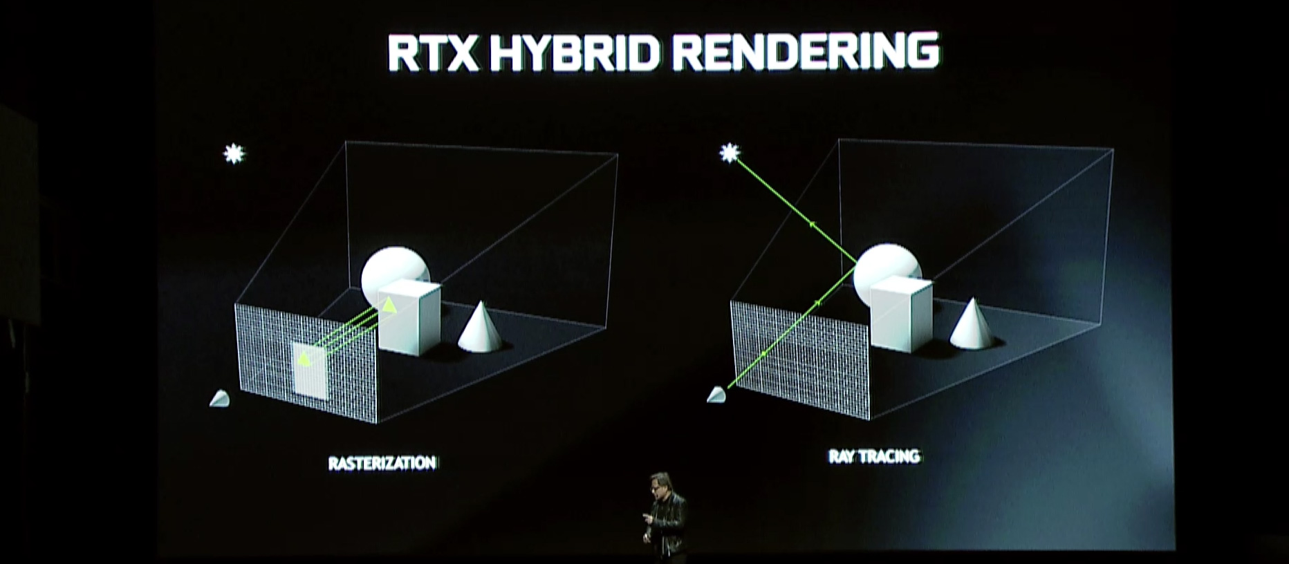
So what does Turing bring to the table? The marquee feature across the board is hybrid rendering, which combines ray tracing with traditional rasterization to exploit the strengths of both technologies. This announcement is essentially a continuation of NVIDIA’s RTX announcement from earlier this year, so if you thought that announcement was a little sparse, well then here is the rest of the story.
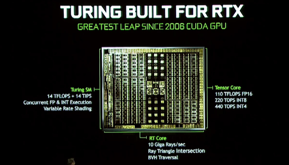
The big change here is that NVIDIA is going to be including even more ray tracing hardware with Turing in order to offer faster and more efficient hardware ray tracing acceleration. New to the Turing architecture is what NVIDIA is calling an RT core, the underpinnings of which we aren’t fully informed on at this time, but serve as dedicated ray tracing processors. These processor blocks accelerate both ray-triangle intersection checks and bounding volume hierarchy (BVH) manipulation, the latter being a very popular data structure for storing objects for ray tracing.
NVIDIA is stating that the fastest GeForce RTX part can cast 10 Billion (Giga) rays per second, which compared to the unaccelerated Pascal is a 25x improvement in ray tracing performance.
The Turing architecture also carries over the tensor cores from Volta, and indeed these have even been enhanced over Volta. The tensor cores are an important aspect of multiple NVIDIA initiatives. Along with speeding up ray tracing itself, NVIDIA’s other tool in their Turing bag of tricks is to reduce the amount of rays required in a scene by using AI denoising to clean up an image, which is something the tensor cores excel at. Of course that’s not the only feature tensor cores are for – NVIDIA’s entire AI/neural networking empire is all but built on them – so while not a primary focus for the Gamescom crowd, this also confirms that NVIDIA’s most powerful neural networking hardware will be coming to a wider range of GPUs.
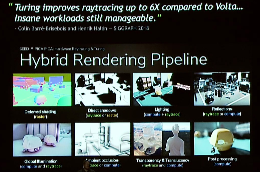
Looking at hybrid rendering in general, it’s interesting that despite these individual speed-ups, NVIDIA’s overall performance promises aren’t quite as extreme. All told, the company is promising a 6x performance boost versus Pascal, and this doesn’t specify against which parts. Time will tell if even this is a realistic assessment, as even with the RT cores, ray tracing in general is still quite the resource hog.
As for gaming matters in particular, the benefits of hybrid rendering are potentially significant, but it’s going to depend heavily on how developers choose to use it. From performance standpoint I’m not sure there’s much to say here, and that’s because ray tracing & hybrid rendering are ultimately features to improve rendering quality, not improve the performance of today’s algorithms. Granted, if you tried to do ray tracing on today’s GPUs it would be extremely slow – and Turing an incredible speedup as a result – but no one uses slow path tracing systems on current hardware for this reason. So hybrid rendering is instead about replacing the approximations and hacks of current rasterization technology with more accurate rendering methods. In other words, less “faking it” and more “making it.”
Those quality benefits, in turn, are typically clustered around lighting, shadows, and reflections. All three features are inherently based on the properties of light, which in simplistic terms moves as a ray, and which up to now various algorithms have been faking the work involved or “pre-baking” scenes in advance. And while current algorithms are quite good, they still aren’t close to accurate. So there is clear room for improvement.

NVIDIA for their part is particularly throwing around global illumination, which is one of the harder tasks. However there are other lighting methods that benefit as well, not to mention reflections and shadows of those lit objects. And truthfully this is where words are a poor tool; it’s difficult to describe how a ray traced shadow looks better than a fake shadow with PCSS, or real-time lighting over pre-baked lighting. Which is why NVIDIA, the video card company, is going to be pushing the visual aspects of all of this harder than ever.
Overall then, hybrid rendering is the lynchpin feature of the GeForce RTX 20 series. Going by their Gamescom and SIGGRAPH presentations, it’s clear that NVIDIA has invested heavily into the field, and that they have bet the success of the GeForce brand over the coming years on this technology. RT cores and tensor cores are semi-fixed function hardware; they can’t be used for rasterization, and the transistors allocated to them are transistors that could have been dedicated to more rasterization hardware otherwise. So NVIDIA has made an incredibly significant move here in terms of opportunity cost by going the hybrid rendering route rather than building a bigger Pascal.
As a result, NVIDIA is attempting a paradigm shift in consumer rendering, one that we’ve really only see before with the introduction of pixel and vertex shaders (DX8 & DX9 era tech) all the way back in 2001 & 2002. Which is why Microsoft’s DirectX Raytracing (DXR) initiative is so important, as are NVIDIA’s other developer and consumer initiatives. NVIDIA needs to sell consumers and developers alike on this vision of mixing rasterization with ray tracing to provide better image quality. And more so than that, they need to ease developers into the idea of working with more specialized, fixed function units as Moore’s Law continues to slow down and fixed function hardware becomes a means to achieve greater efficiency.
NVIDIA hasn’t bet the farm on hybrid rendering, but they’ve never attempted to move the market in this fashion. So if it seems like NVIDIA is hyper-focused on hybrid rendering and ray tracing, that’s because they are. It’s their vision of the future, and now they need to get everyone else on board.
Turing SM: Dedicated INT Cores, Unified Cache, Variable Rate Shading
Alongside the dedicated RT and tensor cores, the Turing architecture Streaming Multiprocessor (SM) itself is also learning some new tricks. In particular here, it’s inheriting one of Volta’s more novel changes, which saw the Integer cores separated out into their own blocks, as opposed to being a facet of the Floating Point CUDA cores. The advantage here – at least as much as we saw in Volta – is that it speeds up address generation and Fused Multiply Add (FMA) performance, though as with a lot of aspects of Turing, there’s likely more to it (and what it can be used for) than we’re seeing today.
The Turing SM also includes what NVIDIA is calling a “unified cache architecture.” As I’m still awaiting official SM diagrams from NVIDIA, it’s not clear if this is the same kind of unification we saw with Volta – where the L1 cache was merged with shared memory – or if NVIDIA has gone one step further. At any rate NVIDIA is saying that it offers twice the bandwidth of the “previous generation” which is unclear if NVIDIA means Pascal or Volta (with the latter being more likely).
Finally, also tucked away in the SIGGRAPH Turing press release is the mention of support for variable rate shading. This is a relatively young and upcoming graphics rendering technique that there's limited information about (especially as to how exactly NVIDIA is implementing it). But at a very high level it sounds like the next generation of NVIDIA's multi-res shading technology, which allows developers to render different areas of a screen at various effective resolutions, in order to concentrate quality (and rendering time) in to the areas where it's the most beneficial.
Feeding the Beast: GDDR6 Support
As the memory used by GPUs is developed by outside companies, there are no big secrets here. The JEDEC and its big 3 members Samsung, SK Hynix, and Micron, have all been developing GDDR6 memory as the successor to both GDDR5 and GDDR5X, and NVIDIA ha confirmed that Turing will support it. Depending on the manufacturer, first-generation GDDR6 is generally promoted as offering up to 16Gbps per pin of memory bandwidth, which is 2x that of NVIDIA’s late-generation GDDR5 cards, and 40% faster than NVIDIA’s most recent GDDR5X cards.
| GPU Memory Math: GDDR6 vs. HBM2 vs. GDDR5X | ||||||||
| NVIDIA GeForce RTX 2080 Ti (GDDR6) |
NVIDIA GeForce RTX 2080 (GDDR6) |
NVIDIA Titan V (HBM2) |
NVIDIA Titan Xp |
NVIDIA GeForce GTX 1080 Ti | NVIDIA GeForce GTX 1080 | |||
| Total Capacity | 11 GB | 8 GB | 12 GB | 12 GB | 11 GB | 8 GB | ||
| B/W Per Pin | 14 Gb/s | 1.7 Gb/s | 11.4 Gbps | 11 Gbps | ||||
| Chip capacity | 1 GB (8 Gb) | 4 GB (32 Gb) | 1 GB (8 Gb) | |||||
| No. Chips/KGSDs | 11 | 8 | 3 | 12 | 11 | 8 | ||
| B/W Per Chip/Stack | 56 GB/s | 217.6 GB/s | 45.6 GB/s | 44 GB/s | ||||
| Bus Width | 352-bit | 256-bit | 3092-bit | 384-bit | 352-bit | 256-bit | ||
| Total B/W | 616 GB/s | 448GB/s | 652.8 GB/s | 547.7 GB/s | 484 GB/s | 352 GB/s | ||
| DRAM Voltage | 1.35 V | 1.2 V (?) | 1.35 V | |||||
Relative to GDDR5X, GDDR6 is not quite as big of a step up as some past memory generations, as many of GDDR6’s innovations were already baked into GDDR5X. None the less, alongside HBM2 for very high end use cases, it is expected to become the backbone memory of the GPU industry. The principle changes here include lower operating voltages (1.35v), and internally the memory is now divided into two memory channels per chip. For a standard 32-bit wide chip then, this means a pair of 16-bit memory channels, for a total of 16 such channels on a 256-bit card. While this in turn means there is a very large number of channels, GPUs are also well-positioned to take advantage of it since they are massively parallel devices to begin with.

NVIDIA for their part has confirmed that the first GeForce RTX cards will run their GDDR6 at 14Gbps, which happens to be the fastest speed grade offered by all of the Big 3 members. We know that NVIDIA is exclusively using Samsung's GDDR6 for their Quadro RTX cards – presumably because they need the density – however for the GeForce RTX cards the field should be open to all of the memory manufacturers. Though in the long run this leaves two avenues open to higher capacity cards: either moving up to 16Gb density chips, or going clamshell with the 8Gb chips they’re using now.
Odds & Ends: NVLink SLI, VirtualLink, & 8K HEVC
While this wasn’t mentioned in NVIDIA’s Gamescom presentation itself, NVIDIA’s GeForce 20 Series website confirms that SLI will once again be available for some high-end GeForce RTX cards. Specifically, both the RTX 2080 Ti and RTX 2080 will support SLI. Meanwhile the RTX 2070 will not support SLI; this being a departure from the 1070 which did offer it.
However the bigger aspect of that news is that NVIDIA’s proprietary cache coherent GPU interconnect, NVLink, will be coming to consumer cards. The GeForce GTX cards will be implementing SLI over NVLInk, with 2 NVLink channels running between each card. At a combined 50GB/sec of full-duplex bandwidth – meaning there’s 50GB of bandwidth available in each direction – this is a major upgrade over NVIDIA’s previous HB-SLI link. This is on top of NVLink’s other feature benefits, particularly cache coherence. And all of this comes at an important time, as inter-GPU bandwidth requirements keep rising with each generation.
Now the big question is whether this will reverse the ongoing decline of SLI, and at the moment I’m taking a somewhat pessimistic approach, but I’m eager to hear more from NVIDIA. 50GB/sec is a big improvement over HB-SLI, however it’s still only a fraction of the 448GB/sec (or more) of local memory bandwidth available to a GPU. So on its own it doesn’t fix the problems that have dogged multi-GPU rendering, either with AFR synchronization or effective workload splitting. In that respect it’s likely telling that NVIDIA doesn’t support NVLink SLI on the RTX 2070.
Meanwhile gamers something new to look forward to for VR, with the addition of VirtualLink support. The USB Type-C alternate mode was announced last month, and supports 15W+ of power, 10Gbps of USB 3.1 Gen 2 data, and 4 lanes of DisplayPort HBR3 video all over a single cable. In other words, it’s a DisplayPort 1.4 connection with extra data and power that is intended to allow a video card to directly drive a VR headset. The standard is backed by NVIDIA, AMD, Oculus, Valve, and Microsoft, so GeForce RTX cards will be the first of what we expect will ultimately be a number of products supporting the standard.
| USB Type-C Alternate Modes | ||||||
| VirtualLink | DisplayPort (4 Lanes) |
DisplayPort (2 Lanes) |
Base USB-C | |||
| Video Bandwidth (Raw) | 32.4Gbps | 32.4Gbps | 16.2Gbps | N/A | ||
| USB 3.x Data Bandwidth | 10Gbps | N/A | 10Gbps | 10Gbps + 10Gbps | ||
| High Speed Lane Pairs | 6 | 4 | ||||
| Max Power | Mandatory: 15W Optional: 27W |
Optional: Up To 100W | ||||
Finally, while NVIDIA only briefly touched upon the subject, we do know that their video encoder block, NVENC, has been updated for Turing. The latest iteration of NVENC specifically adds support for 8K HEVC encoding. Meanwhile NVIDIA has also been able to further tune the quality of their encoder, allowing them to achieve similar quality as before with a 25% lower video bitrate.


223 Comments
View All Comments
Shadyghost - Tuesday, August 21, 2018 - link
Good luck with the lack of support and micro stuttering. I'll never go that route again. I even had games perform worse in sli.mkaibear - Tuesday, August 21, 2018 - link
Intel continuing their tradition of pushing SKUs upmarket, I see. Those prices... eeshk.MrPoletski - Tuesday, August 21, 2018 - link
peak 10 billion rays/s in 250w? not that impressive given that 2 years ago we had measured 100 million rays/s in TWO watts. https://home.otoy.com/otoy-and-imagination-unveil-...eddman - Tuesday, August 21, 2018 - link
I don't see how it's bad. 125 times more power for 100 times better ray tracing performance.Also, that power consumption is for the entire card. The GPU also has a LOT more pixel shaders, so not surprising that it consumes so much more power.
Yojimbo - Tuesday, August 21, 2018 - link
That's a mobile core with 150 GFLOPS of FP32 and probably a memory bandwidth of about 20 GB/s shared between the GPU and CPU. Also, as eddman pointed out, the power consumption you pointed out is only for the SoC and doesn't include the RAM. Power efficiency of mobile SoCs are also much greater than that of high powered chips. BTW, 10 billion divided by 100 million is 100. 100 times 2 Watts is 200 Watts. Now with a mind towards the points I made about the differences between SoCs and high powered graphics cards above, the efficiency of that ImgTec device looks like shit to me in comparison. Maybe we will have a better idea when NVIDIA comes out with a Turing-based Tegra.SydneyBlue120d - Tuesday, August 21, 2018 - link
Is the HDMI still limited to 2.0b? No HDMI 2.1 ?!?!The_Assimilator - Tuesday, August 21, 2018 - link
Nobody cares, since HDMI 2.1-compatible screens and cables are nonexistent. And by the time you can afford 8K these cards will be too slow to drive it.Simon_Says - Tuesday, August 21, 2018 - link
The appeal is not 8k resolution but having UHD + HDR + 4:4:4 + >60fps peak + Adaptive Refresh all on one display.RSAUser - Tuesday, August 21, 2018 - link
These cards don't come close to maxing out the 2.0 standard, so why would you add the extra cost to support the 2.1 standard.euler007 - Tuesday, August 21, 2018 - link
This makes it a hard pass for me, because my next computer upgrade is destined to be hooked up to a large OLED that supports hdmi 2.1 and VRR when such set becomes available (2019 or 2020).