The AMD 2nd Gen Ryzen Deep Dive: The 2700X, 2700, 2600X, and 2600 Tested
by Ian Cutress on April 19, 2018 9:00 AM ESTTalking 12nm and Zen+
One of the highlights of the Ryzen 2000-series launch is that these processors use GlobalFoundries’ 12LP manufacturing process, compared to the 14LPP process used for the first generation of Ryzen processors. Both AMD and GlobalFoundries have discussed the differences in the processes, however it is worth understanding that each company has different goals: AMD only needs to promote what helps its products, whereas GlobalFoundries is a semiconductor foundry with many clients and might promote ideal-scenario numbers. Earlier this year we were invited to GlobalFoundries Fab 8 in upstate New York to visit the clean room, and had a chance to interview Dr. Gary Patton, the CTO.

The Future of Silicon: An Exclusive Interview with Dr. Gary Patton, CTO of GlobalFoundries
In that interview, several interesting items came to light. First, that the CTO doesn’t necessarily have to care much about what certain processes are called: their customers know the performance of a given process regardless of the advertised ‘nm’ number based on the development tools given to them. Second, that 12LP is a series of minor tweaks to 14LPP, relating to performance bumps and improvements that come from a partial optical shrink and a slight change in manufacturing rules in the middle-line and back-end of the manufacturing process. In the past this might not have been so news worthy, however GF’s customers want to take advantage of the improved process.
Overall, GlobalFoundries has stated that its 12LP process offers a 10% performance improvement and a 15% circuit density improvement over 14LPP.
This has been interpreted in many ways, such as an extra 10% frequency at the same power, or lower power for the same frequency, and an opportunity to build smaller chips.
As part of today’s launch, AMD has clarified what the move to 12LP has meant for the Ryzen 2000-series:
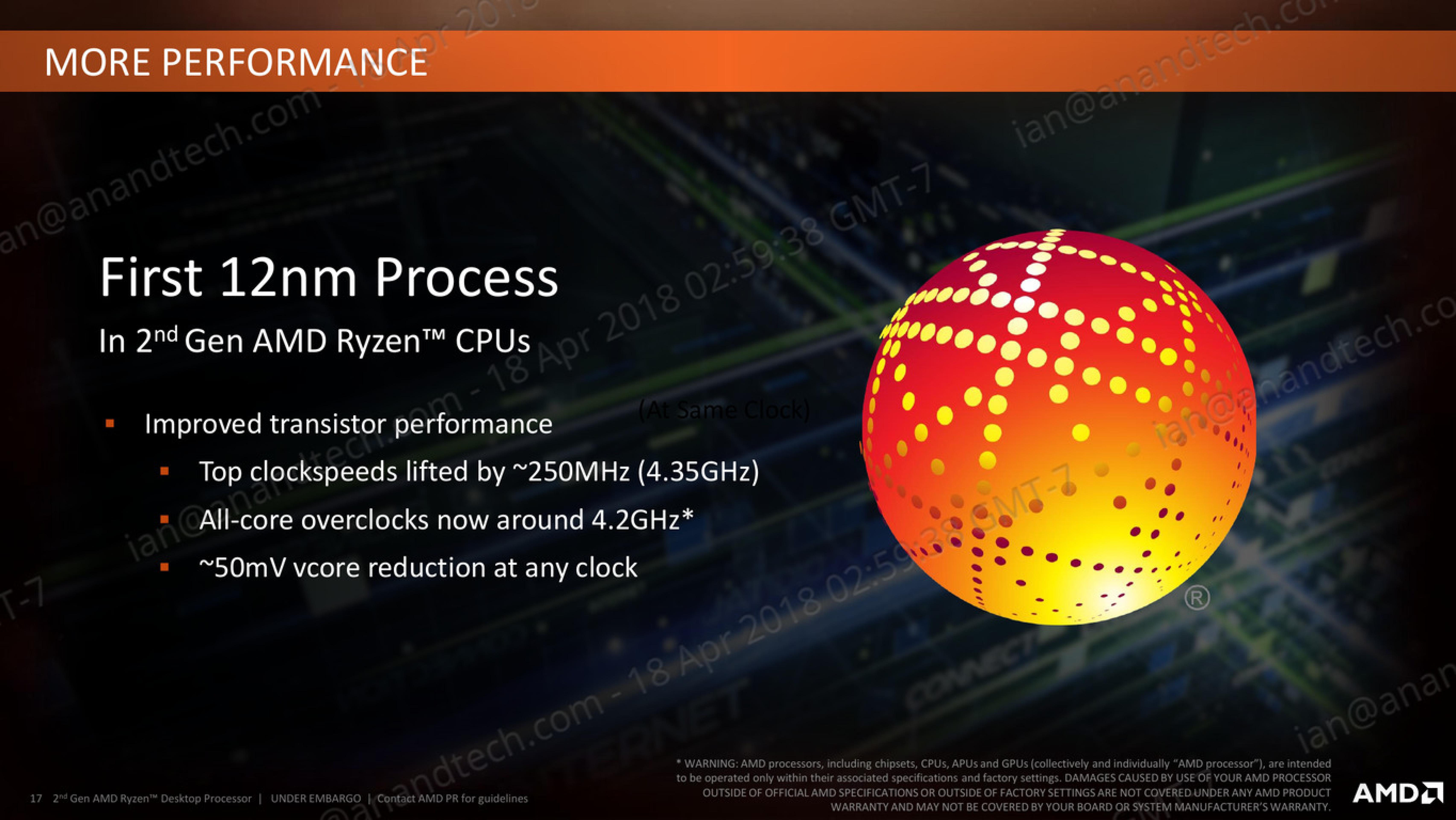
- Top Clock Speeds lifted by ~250 MHz (~6%)
- All-core overclocks around 4.2 GHz
- ~50 mV core voltage reduction
AMD goes on to explain that at the same frequency, its new Ryzen 2000-series processors draw around 11% less power than the Ryzen 1000-series. The claims also state that this translates to +16% performance at the same power. These claims are a little muddled, as AMD has other new technologies in the 2000-series which will affect performance as well.
One interesting element is that although GF claims that there is a 15% density improvement, AMD is stating that these processors have the same die size and transistor count as the previous generation. Ultimately this seems in opposition to common sense – surely AMD would want to use smaller dies to get more chips per wafer?
Ultimately, the new processors are almost carbon copies of the old ones, both in terms of design and microarchitecture. AMD is calling the design of the cores as ‘Zen+’ to differentiate them to the previous generation ‘Zen’ design, and it mostly comes down to how the microarchitecture features are laid out on the silicon. When discussing with AMD, the best way to explain it is that some of the design of the key features has not moved – they just take up less area, leaving more dark silicon between other features.
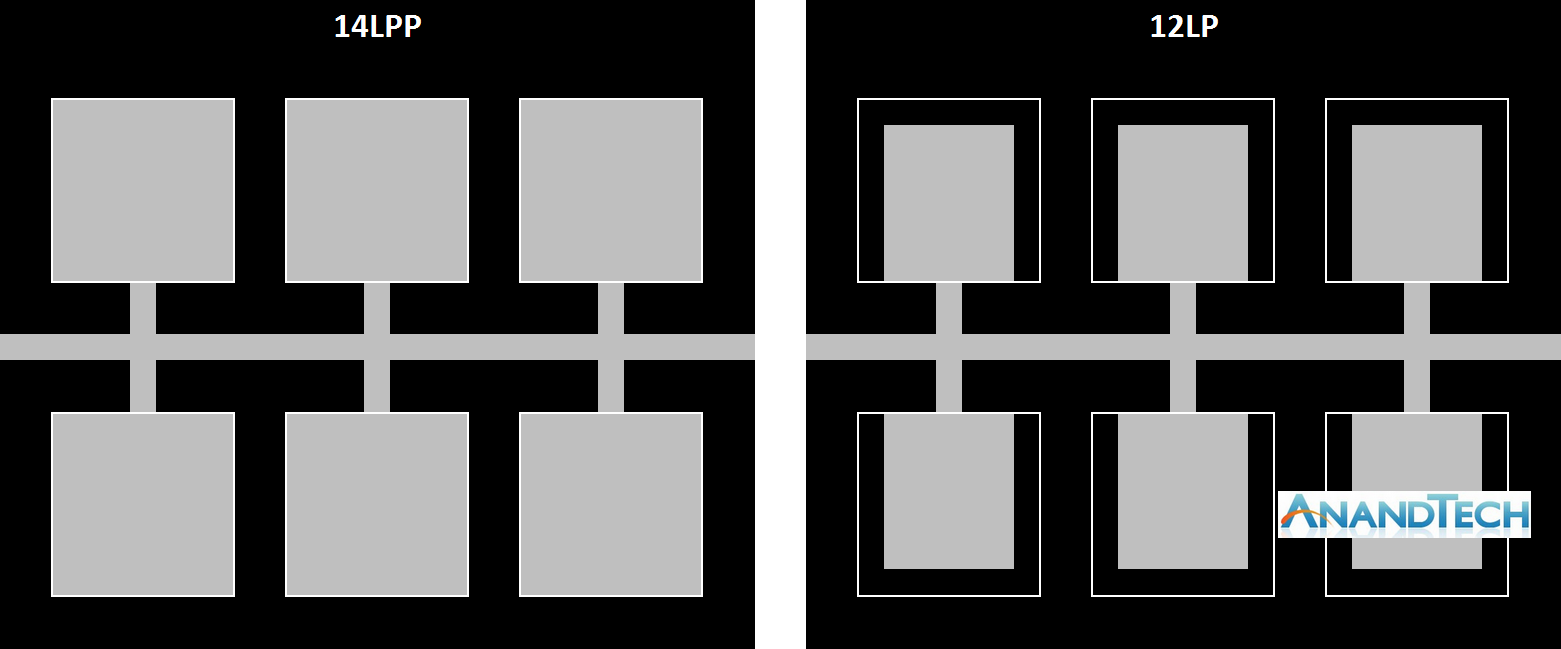
Here is a very crude representation of features attached to a data path. On the left is the 14LPP design, and each of the six features has a specific size and connects to the bus. Between each of the features is the dark silicon – unused silicon that is either seen as useless, or can be used as a thermal buffer between high-energy parts. On the right is the representation of the 12LP design – each of the features have been reduced in size, putting more dark silicon between themselves (the white boxes show the original size of the feature). In this context, the number of transistors is the same, and the die size is the same. But if anything in the design was thermally limited by the close proximity of two features, there is now more distance between them such that they should interfere with each other less.
For reference, AMD lists the die-size of these new parts as 213mm2, containing 4.8 billion transistors, identical to the first generation silicon design. AMD confirmed that they are using 9T transistor libraries, also the same as the previous generation, although GlobalFoundries offers a 7.5T design as well.
So is Zen+ a New Microarchitecture, or Process Node Change?
Ultimately, nothing about most of the Zen+ physical design layout is new. Aside from the manufacturing process node change and likely minor adjustments, the rest of the adjustments are in firmware and support:
- Cache latency adjustments leading to +3% IPC
- Increased DRAM Frequency Support to DDR4-2933
- Better voltage/frequency curves, leading to +10% performance overall
- Better Boost Performance with Precision Boost 2
- Better Thermal Response with XFR2


545 Comments
View All Comments
eek2121 - Thursday, April 19, 2018 - link
Their benchmarks are garbage? You are welcome to buy a 2700X and test for yourself. The benchmarks they used are built in for the most part to each game. It coincides pretty much with what I know of Ryzen, Coffee Lake, and Ryzen 2xxx.AndersFlint - Thursday, April 19, 2018 - link
While out of respect for the reviewer's hard work, I wouldn't describe the results as "garbage", they certainly don't match up with results from other publications.ACE76 - Thursday, April 19, 2018 - link
Yes, Anandtech's are honest and objective...I believe Tech Radar was comparing Coffee Lake OC'd to 5.2ghz vs Ryzen 2700x at 4.1ghz...the stock turbo alone hits 4.3ghz...they are slanting to benefit Intel...a 5.2ghz stable overclock on Coffee Lake alone is very hard to achieve and maybe 10-15% of CPUs can do it.Luckz - Monday, April 23, 2018 - link
I haven't really heard of anyone unable to reach 5 GHz.SkyBill40 - Thursday, April 19, 2018 - link
Well, golly gee... did the other reviewers use the *exact* setup as used here? No? Hmm... I guess that then makes your grouchy mcgrouchface missive not worth consideration then, no? If anyone is to not be taken seriously here, it's you.Typical ad hominem and burden of proof fallacies. Well done, Chris113q.
Flying Aardvark - Thursday, April 19, 2018 - link
WRONG. AT has it right, these are properly patched systems. Heavy IO perf loss with Intel Meltdown patches has been well known for months. See top comment here. https://np.reddit.com/r/pcmasterrace/comments/7obo...Prove your claim that the data is incorrect or misleading in any way whatsoever, child.
RafaelHerschel - Thursday, April 19, 2018 - link
One of the problems is that other reviewers see a less pronounced difference between the new AMD Ryzen CPU's and the older ones. Most reviewers claim that they have tested with all available patches in place.Your conclusion that AT has it right is based on what? Your belief that AT can't make mistakes? Maybe there is a logical explanation, but for now, it seems that AT might have done something wrong.
Flying Aardvark - Friday, April 20, 2018 - link
I have evidence to backup my claim, users with no motivation to mislead agree with AT, and did months ago. You have no evidence, simply butthurt. Good luck.boozed - Thursday, April 19, 2018 - link
Let's ask a total jerk from the internet what he thinks.aliquis - Thursday, April 19, 2018 - link
They definitely used slower memory. Don't know if that's the thing. Don't know what fps others get in the same games and settings. Otherwise maybe it's ASUS doing special tricks like with MCE before or have better memory timits or can use some trick to get similar of precision boost overdrive already. Or a software mistake.Sweclockers is the best for game performance. They do 720p medium so the gpu limits will be smallest there.