The NVIDIA GeForce GTX 1080 & GTX 1070 Founders Editions Review: Kicking Off the FinFET Generation
by Ryan Smith on July 20, 2016 8:45 AM ESTPascal’s Architecture: What Follows Maxwell
With the launch of a new generation of GPUs we’ll start things off where we always do: the architecture.
Discrete GPUs occupy an interesting space when it comes to the relationship between architecture and manufacturing processes. Whereas CPUs have architecture and manufacturing process decoupled – leading to Intel’s aptly named (former) tick-tock design methodology – GPUs have aligned architectures with manufacturing processes, with a new architecture premiering alongside a new process. Or rather, GPU traditionally did. Maxwell threw a necessary spanner into all of this, and in its own way Pascal follows this break from tradition.
As the follow-up to their Kepler architecture, with Maxwell NVIDIA introduced a significantly altered architecture, one that broke a lot of assumptions Kepler earlier made and in the process vaulted NVIDIA far forward on energy efficiency. What made Maxwell especially important from a development perspective is that it came not on a new manufacturing process, but rather on the same 28nm process used for Kepler two years earlier, and this is something NVIDIA had never done before. With the 20nm planar process proving unsuitable for GPUs and only barely suitable for SoCs – the leakage from planar transistors this small was just too high – NVIDIA had to go forward with 28nm for another two years. It would come down to their architecture team to make the best of the situation and come up with a way to bring a generational increase in performance without the traditional process node shrink.
Now in 2016 we finally have new manufacturing nodes with the 14nm/16nm FinFET processes, giving GPU manufacturers a long-awaited (and much needed) opportunity to bring down power consumption and reduce chip size through improved manufacturing technology. The fact that it has taken an extra two years to get here, and what NVIDIA did in the interim with Maxwell, has opened up a lot of questions about what would follow for NVIDIA. The GPU development process is not so binary or straightforward that NVIDIA designed Maxwell solely because they were going to be stuck on the 28nm process – NVIDIA would have done Maxwell either way – but it certainly was good timing to have such a major architectural update fall when it did.
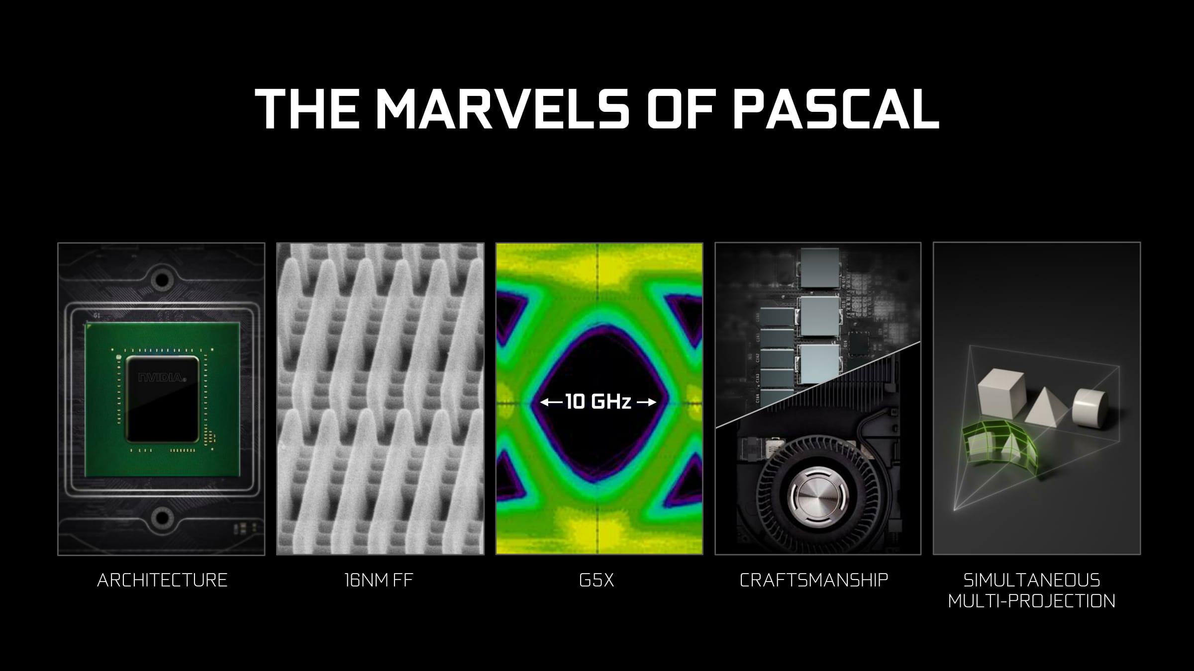
So how does NVIDIA follow-up on Maxwell then? The answer comes in Pascal, NVIDIA’s first architecture for the FinFET generation. Designed to be built on TSMC’s 16nm process, Pascal is the latest and the greatest, and like every architecture before it is intended to further push the envelope on GPU performance, and ultimately push the envelope on the true bottleneck for GPU performance, energy efficiency.
HPC vs. Consumer: Divergence
Pascal is an architecture that I’m not sure has any real parallel on a historical basis. And a big part of that is because to different groups within NVIDIA, Pascal means different things and brings different things, despite the shared architecture. On the one side is the consumer market, which is looking for a faster still successor to what Maxwell delivered in 2014 and 2015. Meanwhile on the high performance compute side, Pascal is the long-awaited update to the Kepler architecture (Maxwell never had an HPC part), combining the lessons of Maxwell with the specific needs of the HPC market.
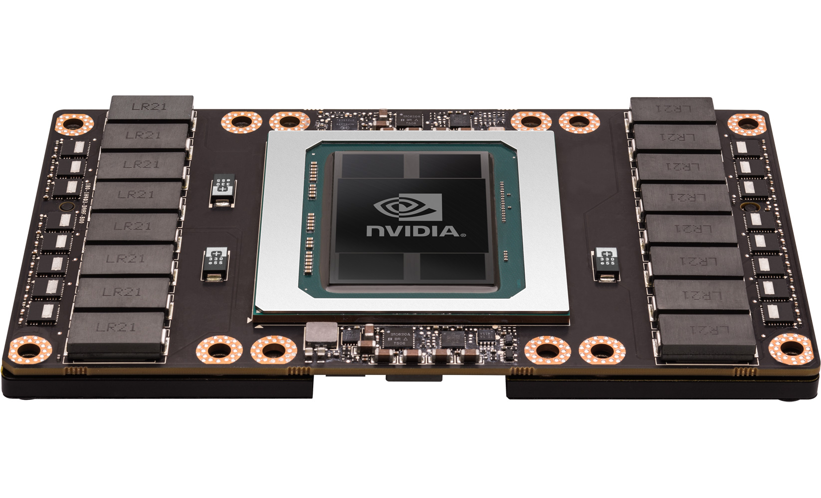
The result is that there’s an interesting divergence going on between the HPC side and its GP100 GPU, and the consumer side and the GP104 GPU underlying GTX 1080. Even as far back as Fermi there was a distinct line separating HPC-class GPUs (GF100) from consumer/general compute GPUs (GF104), but with Pascal this divergence is wider than ever before. Ultimately the HPC market and GP100 is beyond the scope of this article and I’ll pick it up in detail another time, but because NVIDIA announced GP100 before GP104, it does require a bit of addressing to help sort out what’s going on and what NVIDA’s design goals were with GP104.
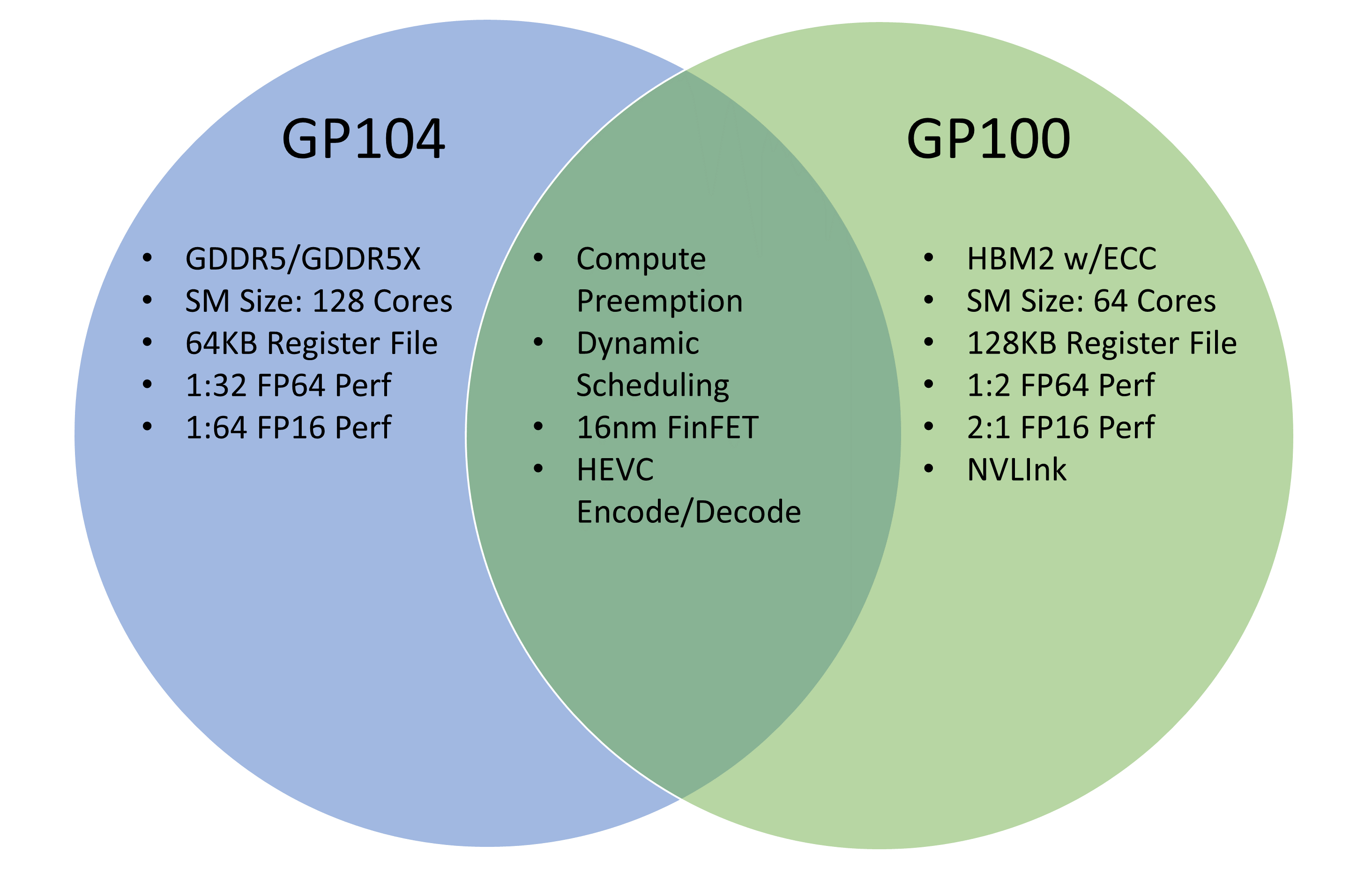
Pascal as an overarching architecture contains a number of new features, however not all of those features are present in all SKUs. If you were to draw a Venn diagram of Pascal, what you would find is that the largest collection of features are found in GP100, whereas GP104, like the previous Maxwell architecture before it, is stripped down for speed and efficiency. As a result while GP100 has some notable feature/design elements for HPC – things such faster FP64 & FP16 performance, ECC, and significantly greater amounts of shared memory and register file capacity per CUDA core – these elements aren’t present in GP104 (and presumably, future Pascal consumer-focused GPUs).
Ultimately what we’re seeing in this divergence is a greater level of customization between NVIDIA’s HPC and consumer markets. The HPC side of NVIDIA is finally growing up, and it’s growing fast. The long term plan at NVIDIA has been to push GPU technology beyond consumer and professional graphics, and while it has taken years longer than NVIDIA originally wanted, thanks in big part to success in the deep learning market, NVIDIA is finally achieving their goals.
This means that although GP100 is a fully graphics capable GPU, it doesn’t necessarily have to be put into video cards to make sense for NVIDIA to manufacture, and as a result NVIDIA can make it even more compute focused than prior-generation parts like GK110 and GF110. And that in turn means that although this divergence is driven by the needs of the HPC market – what features need to be added to make a GPU more suitable for HPC use cases – from the perspective of the consumer market there is a tendency to perceive that consumer parts are falling behind. Especially with how GP100 and GP104’s SMs are differently partitioned.
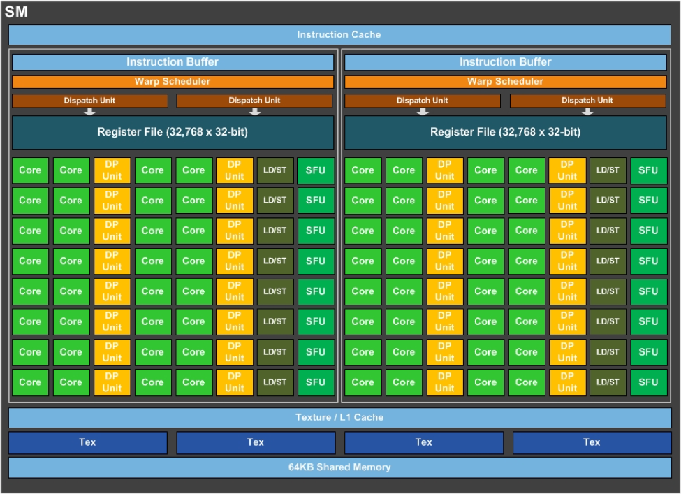
This is a subject I’ll revisit in much greater detail in the future when we focus on GP100. But for now, especially for the dozen of you who’ve emailed over the past month asking about why the two are so different, the short answer is that the market needs for HPC are different from graphics, and the difference in how GP100 and GP104 are partitioned reflect this. GP100 and GP104 are both unequivocally Pascal, but GP100 gets smaller SM partitions in order to increase the number of registers and the amount of shared memory available per CUDA core. Shared memory and register contention on graphics workloads isn’t nearly as great as with HPC tasks – pixel shader threads are relatively short and independent from each other – which means that while the increased ratios benefit HPC workloads, for graphics the gains would be minimal. And the costs to power and die space would, in turn, far outweigh any benefits.


200 Comments
View All Comments
TestKing123 - Wednesday, July 20, 2016 - link
Then you're woefully behind the times since other sites can do this better. If you're not able to re-run a benchmark for a game with a pretty significant patch like Tomb Raider, or a high profile game like Doom with a significant performance patch like Vulcan that's been out for over a week, then you're workflow is flawed and this site won't stand a chance against the other crop. I'm pretty sure you're seeing this already if you have any sort of metrics tracking in place.TheinsanegamerN - Wednesday, July 20, 2016 - link
So question, if you started this article on may 14th, was their no time in the over 2 months to add one game to that benchmark list?nathanddrews - Wednesday, July 20, 2016 - link
Seems like an official addendum is necessary at some point. Doom on Vulkan is amazing. Dota 2 on Vulkan is great, too (and would be useful in reviews of low end to mainstream GPUs especially). Talos... not so much.Eden-K121D - Thursday, July 21, 2016 - link
Talos Principle was a proof of conceptajlueke - Friday, July 22, 2016 - link
http://www.pcgamer.com/doom-benchmarks-return-vulk...Addendum complete.
mczak - Wednesday, July 20, 2016 - link
The table with the native FP throughput rates isn't correct on page 5. Either it's in terms of flops, then gp104 fp16 would be 1:64. Or it's in terms of hw instruction throughput - then gp100 would be 1:1. (Interestingly, the sandra numbers for half-float are indeed 1:128 - suggesting it didn't make any use of fp16 packing at all.)Ryan Smith - Wednesday, July 20, 2016 - link
Ahh, right you are. I was going for the FLOPs rate, but wrote down the wrong value. Thanks!As for the Sandra numbers, they're not super precise. But it's an obvious indication of what's going on under the hood. When the same CUDA 7.5 code path gives you wildly different results on Pascal, then you know something has changed...
BurntMyBacon - Thursday, July 21, 2016 - link
Did nVidia somehow limit the ability to promote FP16 operations to FP32? If not, I don't see the point in creating such a slow performing FP16 mode in the first place. Why waste die space when an intelligent designer can just promote the commands to get normal speeds out of the chip anyways? Sure you miss out on speed doubling through packing, but that is still much better than the 1/128 (1/64) rate you get using the provided FP16 mode.Scali - Thursday, July 21, 2016 - link
I think they can just do that in the shader compiler. Any FP16 operation gets replaced by an FP32 one.Only reading from buffers and writing to buffers with FP16 content should remain FP16. Then again, if their driver is smart enough, it can even promote all buffers to FP32 as well (as long as the GPU is the only one accessing the data, the actual representation doesn't matter. Only when the CPU also accesses the data, does it actually need to be FP16).
owan - Wednesday, July 20, 2016 - link
Only 2 months late and published the day after a different major GPU release. What happened to this place?