Samsung Foundry Updates: 7nm EUV, 10LPP, and 14LPC
by Joshua Ho on April 22, 2016 5:00 AM EST- Posted in
- Samsung
- 28nm
- CMOS
- Semiconductors
- Technology
- 14nm
- 10nm
Earlier this week, Samsung announced a number of updates on the foundry side of their business. While process technology might not be necessarily as interesting as the actual end product from a consumer perspective, it can often give us a good idea for what to expect in terms of performance and power from future products. Of course, it’s up to the various fabless chip design companies around the world to actually exploit the full potential of a process, but in general power and performance are often gated by process node. Almost everything in computing revolves around supporting abstractions, which inevitably means overhead to support these abstractions, so progress at the foundry level is critical for moving the industry forward as a whole.
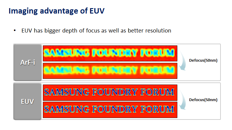
The first, and probably most important announcements are related to process roadmap. The most important point that Samsung made here was that they fully intend to deploy extreme UV (EUV) in mass production for their 7nm processes, which is a pretty significant claim to make as even imec was reluctant to say that EUV would be happening at 7nm. However, those at Samsung seem to believe that this is necessary because otherwise the first metal interconnect layer would require triple patterning, and the transistors themselves would likely be facing similar multiple patterning requirements.
While we’ve discussed EUV before and the challenges that it faces, Samsung believes that triple patterning is not really a viable solution because the number of masks needed goes from roughly 60 or so with double patterning to 90 or so with triple patterning, which results in a steep increase in costs and long lead times for prototypes and production ramp as the masks are made with e-beam lithography for precision, so mispredict penalty for a design isn’t nearly as severe as it would be with a 7nm 193i-only process. Of course, EUV is only going to be used in critical layers, so 193i will still be used for the majority of the layers in the chip, but even so EUV will still be a major hurdle for Samsung to clear here as EUV sources still don’t have enough power to be viable for mass production. Interestingly, Samsung claims that they have mask inspection tools internally for EUV masks, which could help them get to deploying EUV sooner in mass production.
On 10nm, things are less murky as it’s pretty clear that this process will be able to mostly be scaling of the 14nm node to improve performance and possibly improve cost, so the primary update here is that 10LPP (Low Power Plus) will be following 10LPE (Low Power Early) for a 10% improvement in performance. A design done in 10LPE can be directly ported to 10LPP with no new design work.
At 14nm, Samsung seems to be doing well here as their fabs in Korea and Texas are running full time, with over 0.5M wafers shipped and defect density below 0.2 defects/cm^2 in production. This defect density is said to be highly competitive, but I’m not really qualified to say whether this is the case. The primary update of note at 14nm is that 14LPC will have an RF option by the end of the year to enable connectivity for applications like automotive and transceivers.

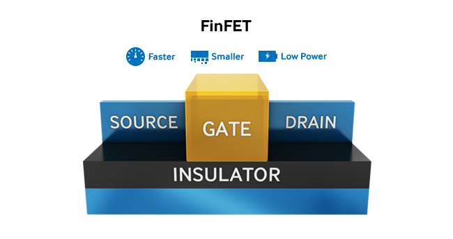
On the process side, 28nm is still pretty critical for a number of applications as this is the last process where planar is viable. Even if 20nm is technically the last planar process, it’s not all that attractive compared to 28nm due to cost, DIBL leakage, and sheer heat density. Samsung’s 28FDS process has been in mass production for some time now as a higher-end node designed to provide ~20nm FinFET class performance on 28nm, but the main news of note here is that 28FDS will have an RF process which adds elements like inductors and is properly characterized to allow for high speed electronics to work properly. 28FDS will also have embedded non-volatile flash memory to enable embedded applications where some memory is needed as a ROM. Kelvin Low of Samsung noted that FD-SOI is also notable for reducing soft error rate relative to bulk CMOS which reduces the need for design-level mitigations, although this was mostly in the context of safety-critical systems that could be seen in automotive and other segments.

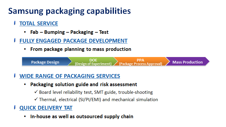
On the design and packaging services side, Samsung is providing more here than before in the form of reference design flows for their 14nm process, and a similar flow will be available for 10nm. Packaging services that used to be for internal use only will also be opened up, with things like 2.5D interposers to enable HBM on GPUs and similar use cases, although it was noted that in that particular case the interposer is currently a bit too expensive for use outside of high-priced components like GPUs. Samsung is also providing some IP blocks for customers to speed up time to market for things like DDR4 and PCI-E controllers.
Overall, Samsung is seems to be quite aggressive on the foundry side and it’ll be interesting to see whether this pays off. Of course, there are the inevitable questions of whether this is comparable to Intel or TSMC’s process, but for now we can’t really say absent details about the pitches of the key layers, operating voltages, and other aspects that we need to consider in order to really compare process nodes. We saw how Samsung’s 14nm push paid off, so it’ll be interesting to see how things shake out with 7nm.
Source: Samsung


54 Comments
View All Comments
watzupken - Saturday, April 23, 2016 - link
With news like this, I think Intel must be panicking. They used to have a good lead over the rest of the fabs, and thus, also gives their chips an edge in terms of performance vs power efficiency. With others catching up with them, that edge is gone and also making their effort to increase market shares vs ARM chips harder.Anymoore - Saturday, April 23, 2016 - link
In 2008, Intel published (link below) that EUV had a fundamental shot noise problem, so that dose would have to keep increasing with smaller size. So source power has to keepincreasing. That's the real reason EUV could never be implemented.http://ieuvi.org/TWG/Resist/2008/022808/simpleEUVS...
Krysto - Sunday, April 24, 2016 - link
So can we expect 10nm from Samsung in the first half of next year, and 7nm by the end of 2019?TC2 - Tuesday, May 3, 2016 - link
I just can't help myself :)Still there is funny peoples with their "AMD will, shall, could, ..."
AMD have nothing significant! They simply can wait someone to give them something :)
---
And now on the matter:
to have X nm process is one thing, to have ability to produce effectively large dies ... is completely different!
---
Live long & prosper !